
Project
The field of 2D materials (2DMs) is just a decade old. Considering the infancy of the field and continuous surprise by the appearance of new 2DMs of different kinds, the physics of these materials is yet to be fully understood. In this respect, we propose to do research on these 2DMs, atomically thin layered quantum materials with an objective to investigate electronic transport in these materials. We believe that high performance electronics need the exquisite materials and immaculate integration process, therefore, the materials and methodologies once established for this domain would certainly be useful for other domains of science and technology.
Our main objective is to develop the high quality electronic devices from 2DMs for practical applications as well as exploring fundamental physics. As identified before, two big challenges related to the 2DMs are: (1) unavailability of high quality materials (2) reproducibility in device integration with these atomic layers. We like to address both of these challenges in this proposal.
Our strategy would be to fabricate the devices from exfoliated as well as from CVD grown flakes. Owing to the pristine nature of exfoliated flakes, these are most desirable for exploring high-end physics, gauging the limit of the material performance and for proof of concept devices.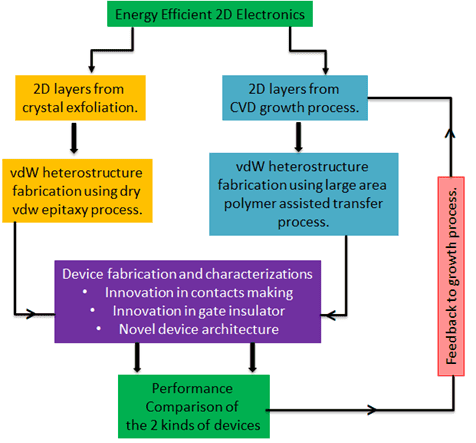
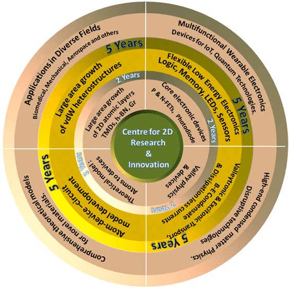
Key objectives of this proposal are identified as below:
- Growth of high quality large area vdW materials and their heterostructures.
- Development of low power flexible electro-optoelectronic devices from these materials.
- Exploring novel physics (novel quantum Degree of Freedom of charge carriers) to produce dissipation less currents.
2DMs based technology can immediately benefit the emerging concepts like IoT in the form of flexible energy efficient sensors. Other sectors where these materials find their immediate use are in bio medical where these are being researched for therapeutic uses and as neural electrodes, in mechanical engineering for light weight composites, in chemical engineering for water filtration and for blue energy to name a few.
Plan of execution of the proposal
Evolution of the proposed plan
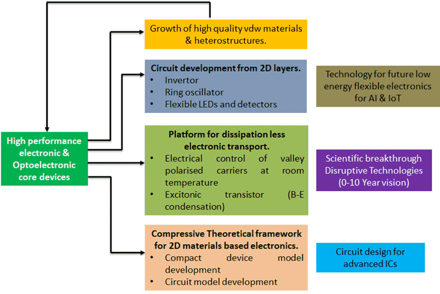
Expected deliverables of the research
- Large area growth of vdW materials and their heterostructures.
- Ultra-low power logic devices including invertor and ring oscillator.
- Low power and high performance flexible devices including LEDs and photo detectors.
- Platform for dissipation less electronic transport (Valleytronic and Excitonic devices).
- High performance and energy efficient electronic and optoelectronic devices.
Current status
The following synthesis and characterization facilities have been installed.
- Two multizone CVD furnaces (one for TMD’s and other for h-BN and graphene).
- High precission 2D material heterostructure assembly set-up.
- A cryogenic electrical probestation ( 78 K to 450 K).
- Dual channel electrical source metere.
- High resolution optical microscope.
- Wetbench with spin coater and hot plate.
The following characterization and simulation tools procurment in progress
- A low temperature micro Raman/Photoluminescence spectrometer
- ATK Quantum Simulator
Established Research Infrastructure
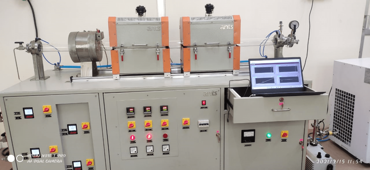
Multizone CVD furnace
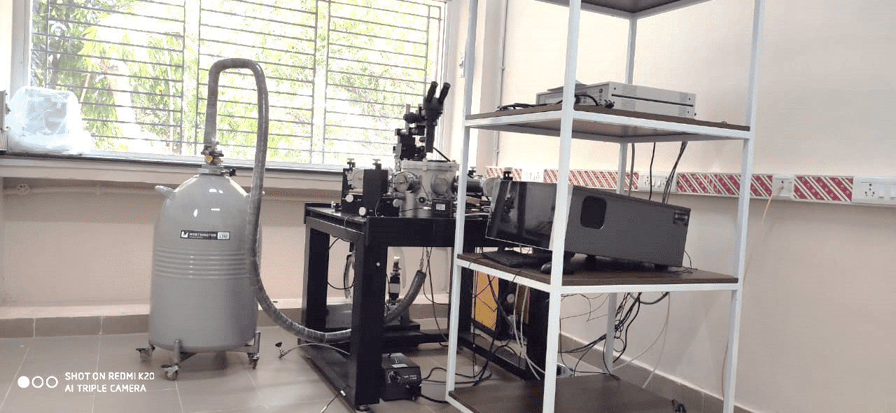
Cryogenic electrical probestation
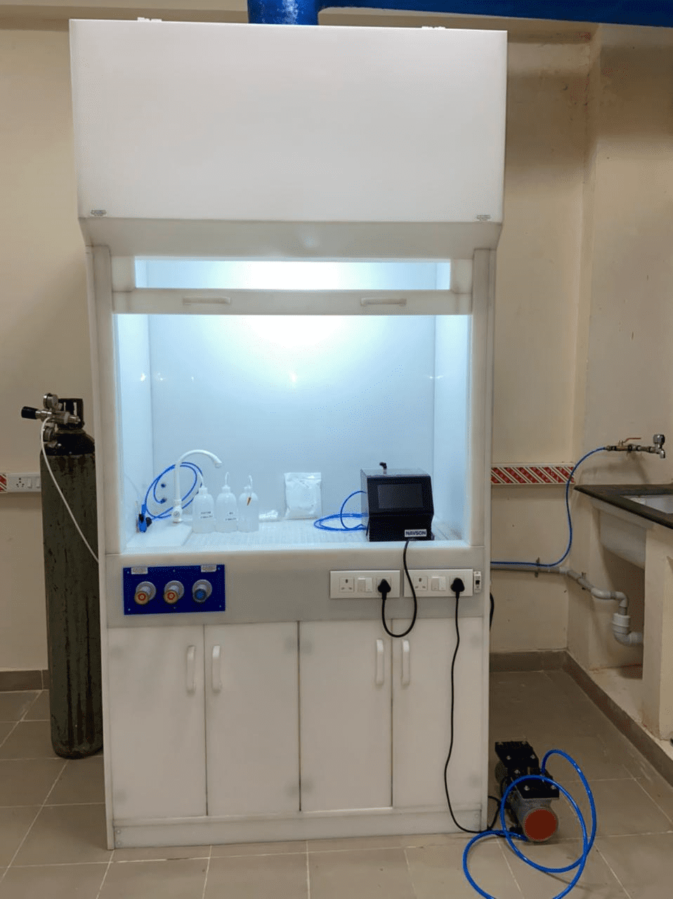
Wetbench with spin coater and hot plate
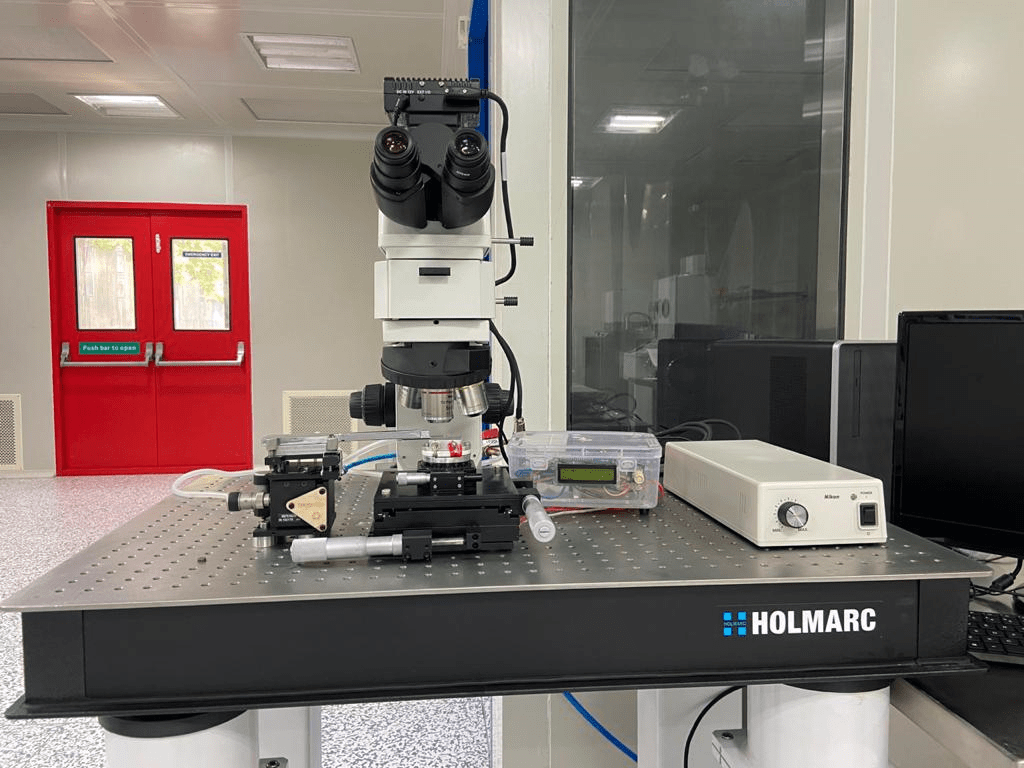
High precission 2D material heterostructure assembly
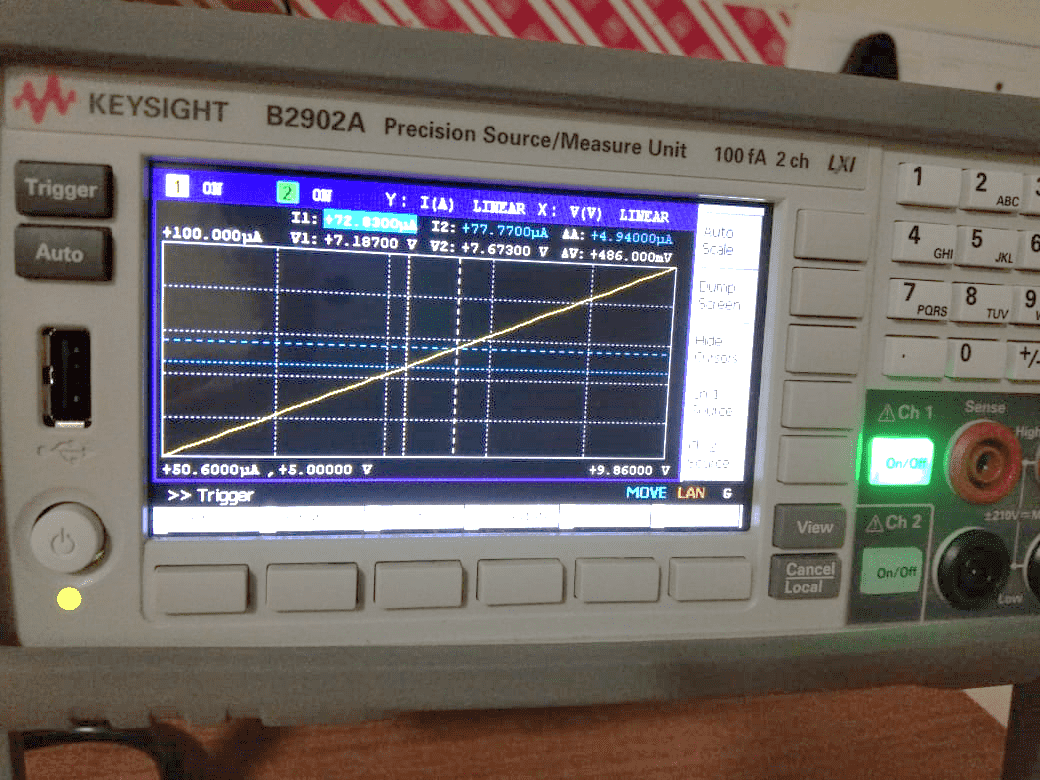
Dual Channel Electrical Source meter
Collaborations
International Advisor
- Prof. Sir Konstantin Novoselov, (Nobel Laureate, Graphene, 2010): University of Manchester, UK and Centre for Advanced 2D Materials, NUS Singapore.
International Collaborators
- Prof. Hyeon Suk Shin, UNIST, Republic of Korea
- Prof. Artem Mishchenko, University of Manchester, UK
- Dr. Maciej Koperski, Assistant Professor, Centre for Advanced 2D Materials, NUS Singapore
- Dr. Jae-Hyun Lee, Assistant Professor, Dept. of Materials Science & Engineering, Ajou University, Republic of Korea
- Dr. Moshe Ben Shalom, Assistant Professor, School of Physics & Astronomy, TEL AVIV University, Israel
- Dr. Ali Esfandiar, Assistant Professor, Department of Physics, Sharif University of Technology, Iran
Industrial collaborations
- M/s Ants Innovations (Mumbai, India)
- M/s Applied Materials ltd (Chennai, India)
External international site links for project
International education programs
Joint Ph.D students :
Ms. Renu Yadav, existing Ph.D scholar in the department of Physics, IITM will be co-guided by Prof. Konstantin Novoselov. Earlier Renu was only guided by Dr. Abhishek Misra.
International workshop ( 2 days): 2D layered Quantum materials: From Physics to Applications
Societal impact
The emerging concept of electronic devices based on vdw materials is expected to deliver high performance light weight, flexible solid state electronic and optoelectronic devices to be used in all frontiers of human life. Newly in-house developed materials will have their potential use in many domains of science and technology. For example in bio medical applications, these materials are being researched for therapeutic uses and electrodes for neural interfaces. The social impact of these materials can be gauged by the ever-increasing demand of such technologies in an attempt to have a better human development index. Therefore, our knowhow of dealing these materials starting from materials growth to device integration would be highly beneficial once the technology culminate and starts giving its results.
Sustenance statement
Advanced materials research is one of the prime thrust area of the Government of India. So, there is high possibility of getting funds from SERB, DST and DietY. We are also aiming to get funding from other government agencies like ISRO and DRDO as they are also looking for new materials and light weight technology. We envision that with the outcomes of this project, we will have monetary support from various IC and optoelectronic industries and semiconductor equipment developer as well as from Government agencies for performing product based research as well as for exploratory research in condensed matter physics.
Technical/ Scientific Progress
New work done in the project
Aiming for the large area growth of 2D materials suitable for scalable technology, we have started to grow various 2D layered semiconductors such as MoS2, MoSe2 and layered insulator hexagonal boron nitride (h-BN). New methodology to grow long strips of MoS2 (~ thickness 3nm) is developed. Physical and electrical characterizations of the as grown material is in progress.
Development of non-volatile flash memory devices using all 2D materials is in progress.
Work function of key topological 2D semimetals is calculated experimentally. Computational based theoretical analysis is performed to corroborate the experimental findings.
We also work on one of the anisotropic TMDs i.e. ReS2, which is among the most ambiguous 2D materials owing to its strong in-plane anisotropy and poor crystal symmetry. Its absolute vibrational feature, among others, is still unclear. We explore the origin of ambiguous peaks that were observed in the Raman spectra of different layer of ReS2. These peaks, unlike the assumptions in literature, are Raman-active in nature and not merely the outcome of defects or interactions with substrate. With the help of first principles DFT, we report layer dependent crystal symmetry in this material. i.e. odd layered ReS2 except monolayer demonstrate symmetry breaking in the structure.
Infrastructure developments
Purchase order to procure RAMAN instrument and low temperature cryostat (~4K) has been issued. We are hoping to get these instruments in 4 months time.
Output
Optimization and integration of ultrathin e-beam grown HfO2 gate dielectrics in MoS2 transistors. K. L. Ganapathi*, N. Bhat and S. Mohan, Journal of Physics D: Applied Physics, 54 (44), 445302 (2021).
Performance Tunability of Field-Effect Transistors using MoS2(1-x) Se2x Alloys. S. Sooraj*, K. L. Ganapathi*, V. Eswaraiah, N.Bhat, Nanotechnology, 32(43), 435202 (2021)
Interlayer excitonic states in MoSe2/MoS2 van der Waals heterostructure. Ankit Arora, Pramoda K. Nayak, Swastibrata Bhattacharyya, Nikhilesh Maity, Abhishek K. Singh, Ananth Krishnan and M. S. Ramachandra Rao. Physical Review B, 103 (2021) 205406 DOI: 10.1103/PhysRevB.00.005400.
Study of Thermal Conductivity in Two-dimensional Bi2Te3 from Micro-Raman Spectroscopy Manavendra P. Singh, Sumarlang Ryntathiang, Sivarama Krishnan, Pramoda K. Nayak. Current Chinese Science (2021) DOI: 10.2174/2210298101666210412101104
Work Function of van der Waals Topological Semimetals: Experiment and Theory. Under review in Applied Physics Letters.
Review of Quantum emitters and detectors based on 2D vdW Materials by Madhura G. Dastidar, Immanuel Thekkooden, Pramoda K. Nayak, Vidya P. Bhallamudi Under Review ( 2021)
Talks/Presentations:
Dr. Abhishek gave an invited talk in the Workshop on 2D Materials: Fundamentals to Applications organised by Department of Physics and Nanotechnology, SRM Institute of Science and Technology, Chennai.
Dr. K.L. Ganapathi gave an Invited talk at 3rd Indian Materials Conclave and 32nd Annual General Meeting of MRSI (December 20-23, 2021) Title: “2D layered Semiconductors and Oxide Heterostructures: Physics and Applications”
Study of polarization and layer dependent Raman modes in anisotropic ReS2. P. Upadhyay, N. Maity, P. K. Barman, R. Kumar, A. K. Singh, P. K. Nayak. Oral presentation at the 12th Recent Progress in Graphene and Two-dimensional Materials Research Conference (RPGR 2021), Yonsei University, Seoul, South Korea (October 2021).
Twist angle dependent higher order excitations in van der Waals Heterostructures Pramoda K. Nayak Webinar on Nanotechnology and Nanomedicine, PHRONESIS LLC, USA (March, 2021)
Tunable exciton-trion state in twisted bilayer WSe2 Pramoda K. Nayak, Prahalad Kanti Barman, Pranshoo Upadhyay, Global Virtual Summit on Carbon, Graphene, 0D, 1D, and 2D Materials (July, 2021) (best presentation award)
Layer Dependent Semiconductor to Metal Transition in PtSe2: From First Principle Calculation Vishal K. Pathak, N. Meenakshisundaram and Pramoda K. Nayak 65th DAE Solid State Physics Symposium (DAE-SSPS 2021) held at Mumbai during December 15-19, 2021.
Chirality sensitive Raman modes and in-plane anisotropy in α-MoO3 Ravindra Kumar, Prahalad K. Barman, M. S. Ramachandra Rao, Pramoda K. Nayak Third Indian Materials Conclave and the 32nd Annual General Meeting of MRSI, held at IIT Madras, December 20-23, 2021
Mobility
Visits planned for PI, co-PIs, international collaborators and students (both inbound and outbound)
Ph.D scholar Mr. Saroj Poudyal and Miss Renu Yadav is planning to visit University of Manchester, UK and National University of Singapore in summer 2022. Proposals to support these travels are submitted under HRHA travel grant of IITM.
Relationship
Industrial Engagement
We are working with Ants Innovations Pt. Ltd. to develop the CVD furnace for large area growth of 2D materials.
University Engagement
Nobel Laureate Prof. Konstantin Novoselov is agreed to be a co-guide of Ph.D scholar Miss Renu Yadav. Prof. Novoselov is currently working in the Graphene Research Centre, NUS Singapore.
Prof. Artem Mischenko from University of Manchester, UK is agreed to be a co-guide of Ph.D scholar Mr. Saroj Poudyal.
A joint proposal from Aalto University (AALTO), University of Jyväskylä (Finland Node), and IIT Madras and IIT Kharagpur (India Node) is submitted under The Global Programme Pilots from the Ministry of Education and Culture (MEC) Finland-India.