


Project
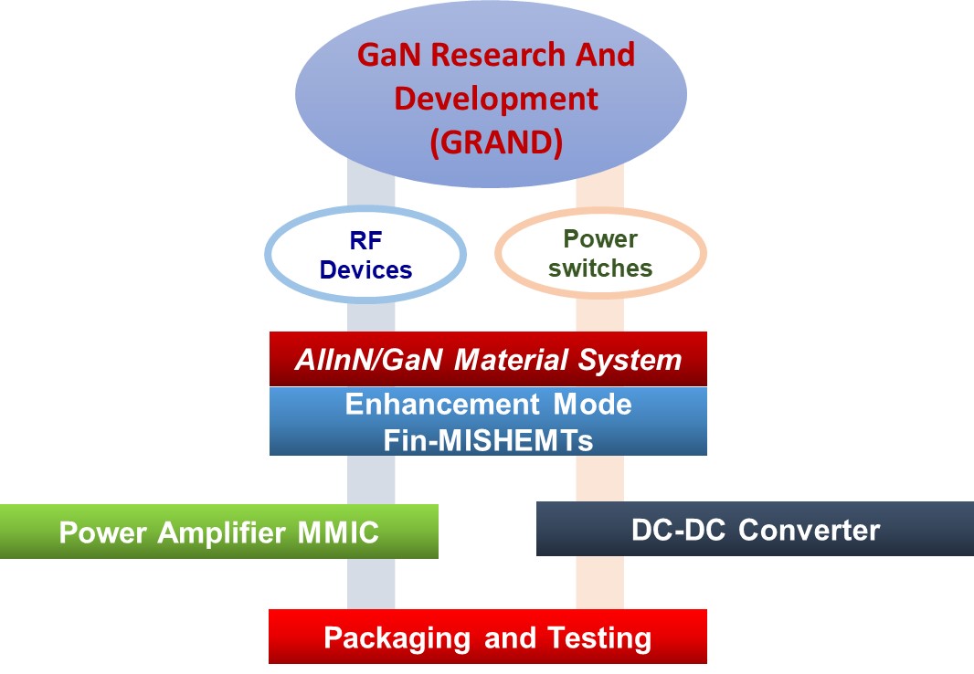
In Phase -1, greater emphasis will be on development of reliable e-mode HEMTs, their characterization and modelling. The threshold voltages of the HEMTs will be controlled by designing the geometry of MIS-FinFETs and controlling the charge in the gate dielectric deposited by Reactive Ion Sputtering (RIS). As we already have some success on tailoring the threshold voltage by engineering the charge in the Al2O3 layer deposited by RIS, we are confident of achieving reliable e-mode devices with this process within two years. The devices will be characterized and the model parameters will be extracted, which is very important for designing the power amplifier and switching circuits. Design of Power Amplifier and power switching circuits will also be carried out at this stage.
In Phase -2, the emphasis will be on development of power amplifier MMICs and power switches for specific applications using the e-mode HEMTs developed in the earlier phase. In addition, research work will also be carried out to realize e-mode MIS-FinFETs using gate dielectrics deposited by Atomic Layer Deposition (ALD), their characterization and modelling. ALD is the industry-standard technique for deposition of thin films and we would like to compare the quality of the sputter-deposited films with ALD. It should be noted that so far there is no report of successful charge engineering by ALD. However, we have some ideas about how to incorporate charges in the dielectric deposited by ALD. This can be a more robust process and can lead to very high impact publications/patents and technology transfer.
GaN device development:
To meet the requirements of PA and power switches, significant enhancement in device performance is required. We plan to take the best features of the process flows already developed in our laboratory and fabricate MIS-FinHEMTs to achieve e-mode devices with charge-engineered gate dielectric. Also the fin geometry has to be carefully tailored to modulate Vth and achieve reduced Ron. Therefore considerable work is required in the following areas:
- Ohmic contact optimization:
- Optimization of gate dielectric deposition process:
- Realization of Fins by dry etching
- Gate patterning by E-beam lithography
- SiNx passivation
- Process Integration of active and passive components
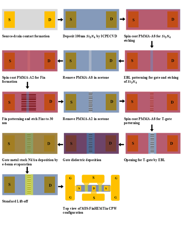
Proposed process flow for MIS-FinHEMT
Model development :
This involves a significant extension of a static HEMT model already developed at our group. This process requires formulating new models to cater new effects such as the change in threshold voltage, effects of traps, gate leakage on the static characteristics etc. Apart from that a dynamic charge model has to be developed as well. A significant effort will be spent on the model development to cater to the static and dynamic electrothermal behavior, which is important in case of power amplifier design. The goals and deliverables of this compact modeling are three-fold:
- To develop and implement the compact models within circuit simulators,
- To extract model parameters and
- To validate the model for DC, CV and RF operations with measured characteristics of fabricated devices
Characterization :
The purpose of device characterization is three fold:
- Regular monitoring of device performance and gives proper feedback to process and device development
- Extraction of parameters for model development
- Test device degradation under accelerated and long duration stress for reliability qualification The first job involves definition and design of test structures where all the above characterization can be done. The test structures involve HEMT designs with various width, gate length, drain-gate, gate-source spacing to measure transistor performance, passive structures like capacitor, inductor, structures for parasitic resistance and capacitance measurements. The test chip in the initial development phase will contain a lot of parametric variations. During the subsequent phases, these variations will be reduced, few would be selected and placed in large numbers to check yield. There will be special test structures for RF measurement and reliability tests.
Power Amplifier MMIC development :
The PA commercial IC space is presently covered by LDMOS (low-cost, low-frequency, medium power), GaAs (medium cost, high frequency, medium power) and d-mode GaN (high cost, medium frequency, high power). The high-power space is dominated by d-mode GaN devices that require negative gate voltage biasing, and a separate associated bias controller chip. There is thus a huge commercial and strategic potential for the use of e-mode GaN devices, which do not require a separate biasing IC.
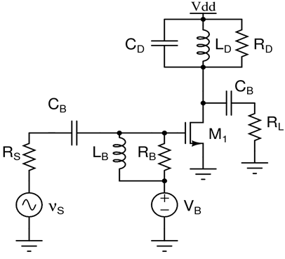
A representative circuit diagram of the PA
Components for Power switching
Power electronics industry is looking for potential devices which can replace Si MOSFETs. Today all the system level attempts in the power electronics industry is towards making energy efficient and compact power converters. Usage of GaN HEMT based e- mode devices will give a major boost to the power electronics industry.
In the low voltage and low power segment, applications like mobile battery charger, battery charger for automotive applications, low voltage DC-DC power supplies will find tremendous usage of GaN HEMT devices. A gate driver is an electronic interface between power devices and control circuits. A reliable operation and protection of these devices largely depends on appropriate design of a suitable gate driver circuit. In this project, a suitable gate driver circuit to drive the GaN devices will be developed. Also with the gate driver the developed GaN device will be used in a power converter application. One of the typical applications of 1 kW battery charger can be targeted for this purpose.
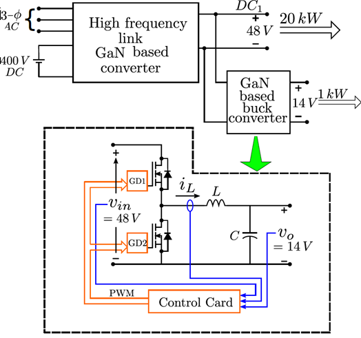
Block diagram of the 20 kW automotive power supply
Expected deliverables of the research
The target specifications for HEMTs for Power Amplifier applications are:
- Drain current : > 500 mA/mm for enhancement mode devices
- Threshold Voltage: 0 to +2 V
- Threshold voltage stability: within ± 300 mV for full gate swing (-50°C to +200°C)
- Cut-off frequency: > 80 GHz
- Breakdown Voltage: > 60V
- Transconductance: > 300 mS/mm
- Output power: > 5 W/mm
- Gate leakage: < 100 nA/mm
- Dynamic Ron/static Ron : 1.05 to 1.1 for VDS0 = 40 V
- Temperature range of operation: -50°C to 200°C
The target specifications for HEMTs for Power switching applications are:
- Output Power: 1 kW.
- Nominal input voltage: 48 Volts
- Minimum input voltage: 40 Volts.
- Maximum input voltage: 60 Volts.
- Nominal output voltage: 14 Volts.
- Output current: 72 Ampere.
- Typical expected switching frequency for these applications: 1 MHz.
- Typical switch rating required for this application is as follows: 100 Volts, 25 Ampere. We will parallel 4 such devices at the first stage.
- Continuous rating: 100 Volts/30 Ampere.
- On state resistance Rds (on): 20 mOhm.
- Switching time (turn on and turn off): < 10 ns.
- Operating temperature: -40 C to 150 C
The specifications of a single-chip PA MMIC that can be developed in this project are:
- Frequency: 5GHz
- Saturated Output power: 10W
- Supply voltage: 28V
- Power Added Efficiency: 20%
- Power Gain: 20dB
- Input Return loss: > 6dB
- Bias current: 2A
The specification of the battery charger are:
- Output Power: 1kW.
- Nominal input voltage: 48 Volts
- Minimum input voltage: 40 Volts.
- Maximum input voltage: 60 Volts.
- Nominal output voltage: 14 Volts.
- Output current: 72 Ampere.
- Typical expected switching frequency for these applications: 1 MHz.
- Typical switch rating required for this application is as follows: 100 Volts, 25 Ampere. We will parallel 4 such devices at the first stage.
- Continuous rating: 100 Volts/30 Ampere.
- On state resistance Rds (on): 20 mOhm.
- Switching time (turn on and turn off): < 10 ns.
- Operating temperature: -40 C to 150 C.
Current status
MIS-FinHEMT fabrication
- MIS-FinHEMT with submicron gate length and SiN gate dielectric has been fabricated and the characterization is in progress
Passive elements
- Inductors are being designed and fabricated
Compact model of MIS-HEMTs
- Static model has been developed
- Dynamic model is in progress
Characterization and extraction of parameters
- Ongoing
Power amplifier design
- In progress
Collaborations
University of Limoges, France
- We have a strong ongoing Indo-French collaboration in the area of GaN-based devices. IIT Madras and University of Limoges have already signed an MOU in October 2018.
Industrial collaborations
- Veeco Instruments Inc., USA
- XLIM, France
- SSPL, India
International education programs
- An Indo-French workshop was approved under the aegis of CEFIPRA and several speakers from industries e.g. AMCAD, UMS and OMMIC as well as from academia had agreed to participate. Due to the covid-19 pandemic we now plan to hold it in February 2022.
Societal impact
A major contribution of GaN technology is in the area of power electronics. It is extensively used in the area of power converters, e.g. laptop chargers/ mobile chargers/Automotive battery chargers with considerable power saving. Power Electronics industry is always in search of ideal devices with zero switching time and zero conduction loss. However currently used Si devices have their own limitations for the same. On the contrary, GaN devices show a lot of promise, which will allow the device size to shrink by at least 10 times. Due to that, converter size will be reduced dramatically and efficiency will improve to a great extent. Therefore it is high time to develop GaN based devices indigenously so that India becomes independent in this aspect, too. This can have a very strong societal impact. Moving from normally ON to normally OFF (e-mode) devices will further improve the power efficiency of the circuits. Hence GaN based e-mode HEMT technology can play an important role in the development of green buildings and cities. Another important application of GaN HEMT technology is in the area of high power and high frequency electronics. It will play a major role in communications systems for 5G and 6G in future. Our proposed development of power amplifiers is a step in that direction. GaN based MMICs are also attractive for a wide variety of defense requirements, such as transmitter/ Receiver (T/R) modules for Radar applications, power amplifiers for satellite communication and smart weapons and wide band high power amplifier modules for electronic warfare systems.
Sustenance statement
The research activity in the area of GaN- devices will continue in collaboration with Centre for NEMS and Nanophotonics (CNNP). We already have a protocol in place by which external agencies are using CNNP facilities for their research on payment basis. This will help us generate funds to sustain the Centre. Apart from this, we also plan to get new projects in this area regularly. We have already completed one exploratory project sponsored by SSPL in this area and expect a long-term commitment from them to address the defense requirement of the country. We have started some collaboration with SCL, Chandigarh through a DST project and we hope to strengthen our collaboration in the area of GaN research through new projects. It has already been mentioned that there is a big requirement to educate Power Engineers regarding the advantages and potential of GaN based HEMTs in power electronics. We shall conduct regular Workshops for People from Industry, which can generate revenue for the Centre