


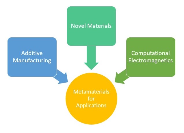
Project

Examples of existing capabilities in the simulation, design, fabrication, and testing of additively manufactured antennas, of components, of metamaterials, and of a material characterization setup.
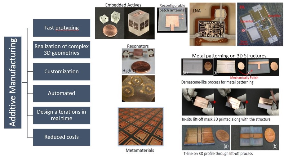
3D printed wideband antenna
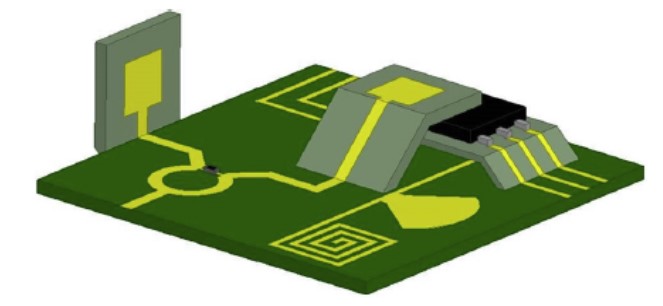
An ultrawideband Vivaldi antenna with a structurally embedded receive module is fabricated using a combination of 3-D printing and thin-film processes.
A rigid-flex fabrication technique is adopted here to design a receive module. This technique utilizes Rogers 3850HT [liquid crystal polymer (LCP)] flex and 3-D printed rigid structures to fabricate the antenna and its feed.
The measurements of this 3-D printed system-on-antenna (SoA) front-end module shows 5-dB more receive power compared to the ridged horn antenna-based design. This improvement is due to the absence of long transmission lines and connectors in the 3-D printed design.
A low-cost, lightweight, and high functional density system with improved performance can be achieved through 3-D printing.
(left) The receive module is placed in a packaging cavity that is formed in the unused region of the antenna structure. (right) Final package with cap covering the cavity. This package also has the added benefit of providing isolation for the receive circuit.
Cost effective light-weight spherical cavity using polyjet 3D printing technology
Two hemispherical resonator parts are 3D printed using a photopolymer resin material and a commercially available polyjet printer. The inner surfaces of the cavities are metalized with a layer of 15 m thick copper using electroplating.
A 35 m thick magnetic nanoparticle film deposited on a LCP host substrate is placed at the center of the 3D printed cavity where the magnetic fields are the strongest.
Two 3D printed dielectric rods are used to suspend and rotate the film to achieve very fine frequency tuning. The two cavity parts are then assembled through a lego-like process. The whole package is 60 gm in total weight.
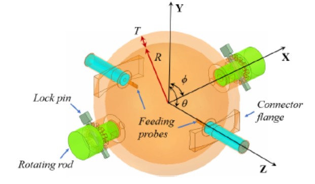
The electrically excited air-filled cavity resonator with rotating rods (magnetic film is not shown for clarity). R = 16 mm, T = 3 mm.
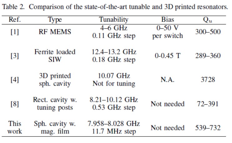
The tuning range can be increased by improving the magnetic nanoparticle fill factor in the film and choosing a ferrite material with a higher r.
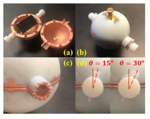
Fabricated samples:(a) metalized cavity parts with magnetic film placed,(b)fully assembled cavity resonatorator,(c) enlarged picture of corrugated rod sleeve,(d) Two rotated positions
Out-of-Plane Antennas with 3D printing
3D printing, unlike micromachining, does not involve complicated steps in the fabrication and uses few fabrication tools making it a fast, cost-effective, accurate, and a repeatable process. The use of the air-gap approach to design antenna substrates allows overcoming the performance limitations due to losses associated with the substrate.
Figure presents the application of 3D printing in designing a complex high-density packaging solution for a microwave system with an integrated out-of-plane patch antenna.
In the future, using 3D printing, more complex design such as frequency dependent reflectors can be fabricated and can be used to achieve additional functionalities such as multiple frequency bands for better impedance matching and a smaller front-to-back ratio.
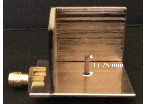
Monopole antenna with a reflector
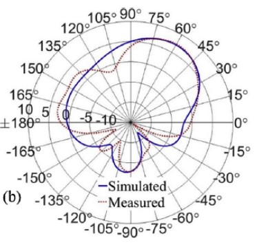
Simulated and measured radiation patterns.
The major advantage of using 3D printing for fabricating Yagi-Uda antennas is that the directors of different height can readily be fabricated in comparison to a traditional micromachining process.
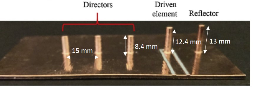
Vertical Yagi-Uda antenna
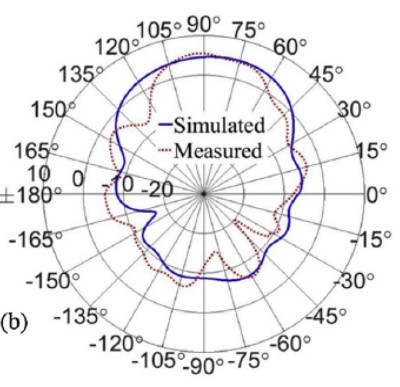
Simulated and measured radiation patterns.
Bidirectional, Bandwidth-Enhanced Metamaterial Absorber for Microwave Applications
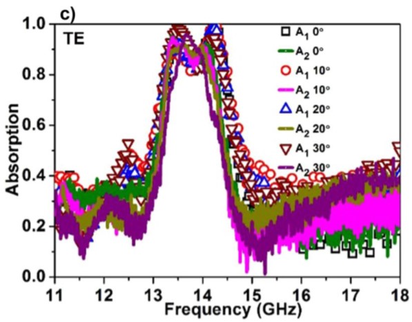
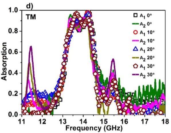
A bidirectional bandwidth-enhanced absorber is realized with a unit cell having basic metallic elements such as strips and squares optimized to have adjacent resonances leading to a bandwidth-enhanced absorption. The optimized bidirectional absorber exhibits absorption greater than 90% from 13.38 GHz to 14.4 GHz along one direction, and in the reverse direction, it exhibits near perfect absorption between 13.40 GHz and 14.25 GHz.
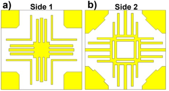
The optimized design of the bidirectional bandwidth-enhanced absorber is fabricated on FR-4 board with 267.8 mm × 267.8 mm × 1.5 mm dimensions
Owing to the four-fold symmetry of the constituting metallic patterns, the absorber maintains bidirectional bandwidth-enhanced absorption for both transverse electric (TE) and transverse magnetic (TM) polarizations.
The structure is polarization insensitive and wide-angle receptive, which maintains bandwidth-enhanced nature as well as high magnitude up to 30°.
Vertical Yagi-Uda antenna
Simulated and measured radiation patterns.
Chiral metamaterial (CMM) for broadband asymmetric transmission (AT) of linearly polarized EM waves
A metal-dielectric-metal configuration with simple complementary strips as resonant elements is proposed for the broadband AT. The slanted metallic patterns on the front and back layers are orthogonal breaking the symmetry in the propagation direction. The whole chiral medium exhibits AT due to the strong electric and magnetic cross coupling generated in the structure.
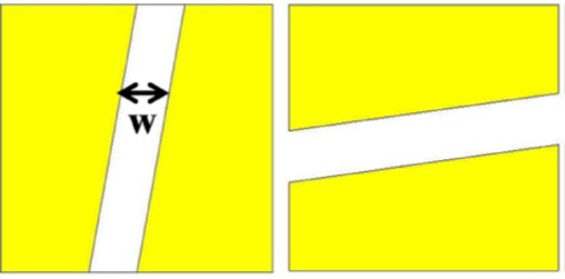
The unit cell of the proposed AT CMM with dimensions 11.5mm 11.5mm, and thickness 0.787mm. The gap dimension (w) in the front and back metallic structure is 2.2mm. The metal patterns are realized with copper of thickness 0.034mm and a conductivity of 5.8 107 S/m.
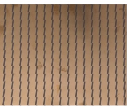
The AT structure is fabricated on a Rogers RT5880 board (𝜀_𝑟=2.2, loss tangent 0.0009) using standard printed circuit board techniques with the periodic pattern consisting of 1919 unit cells.
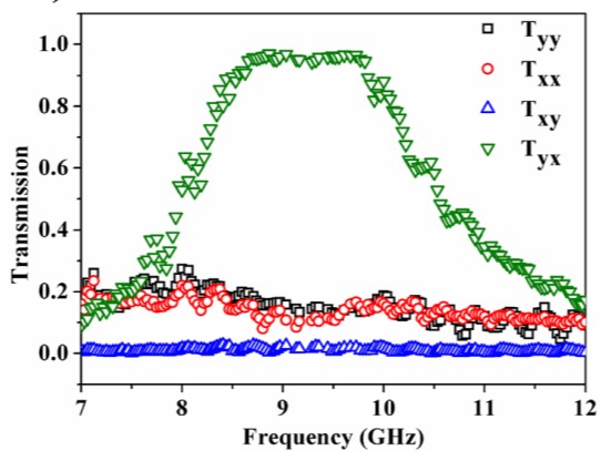
Measured transmission parameters in the forward direction for x- and y- polarization states
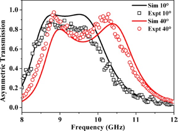
Comparison of simulated and measured angular variation of asymmetric transmission.
Tailoring Antenna Focal Plane Characteristics for a Compact Free-Space Microwave Measurement Setup
A compact setup (4λc–8λc) with custom-designed dielectric lenses is fabricated and tested. Permittivity extraction is demonstrated on low and high loss MUTs of sizes 10λc × 10λc or of sizes as small as 3.3λc ×3.3λc using appropriate lenses. Errors are less or comparable with classical method.
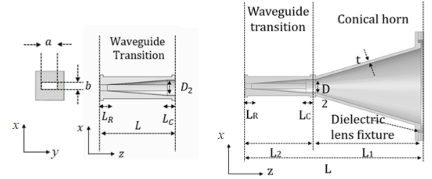
Cut views of the waveguide mode converter, and full model.
A waveguide mode converter was designed and fabricated to convert the TE10 mode within the rectangular waveguide to the TE11 mode.A conical Horn antenna was designed to couple with the converter and achieve 20-dB radiated gain. Three dielectric lenses with loose and tight focal lengths were designed, fabricated and evaluated.
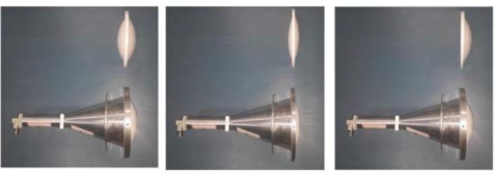
Horn and converter with (a) tight focusing biconvex lens 1, (b) loose focusing biconvex lens 2, and (c) loose focusing plano-convex lens 3.
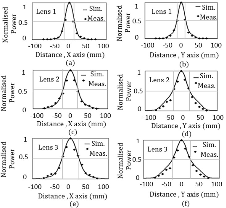
Measurements of focal plane characteristics done using a printed E-field sensor
Efficient Acceleration Scheme
The present proposal seeks to design metamaterial lenses, absorbers and metasurfaces through a variety of computational tools.
The analysis of fields in periodic dielectric structures arise in numerous applications of recent interest, ranging from photonic bandgap structures and plasmonically active nanostructures to metamaterials. To achieve an accurate representation of the fields in these structures using numerical methods, dense spatial discretization is required. An example of the implementation of an acceleration scheme developed at MSU is depicted.
Full-wave solutions would be generated, using commercial FEM and FDTD based tools, to a limited extent due to constraints on computational resources.
Efficient algorithms, developed within the group, and through R&D, are planned.
On-going work at IITM on the use of geometric optics, transformation optics and lumped element based designs would be extended through the collaboration with MSU.
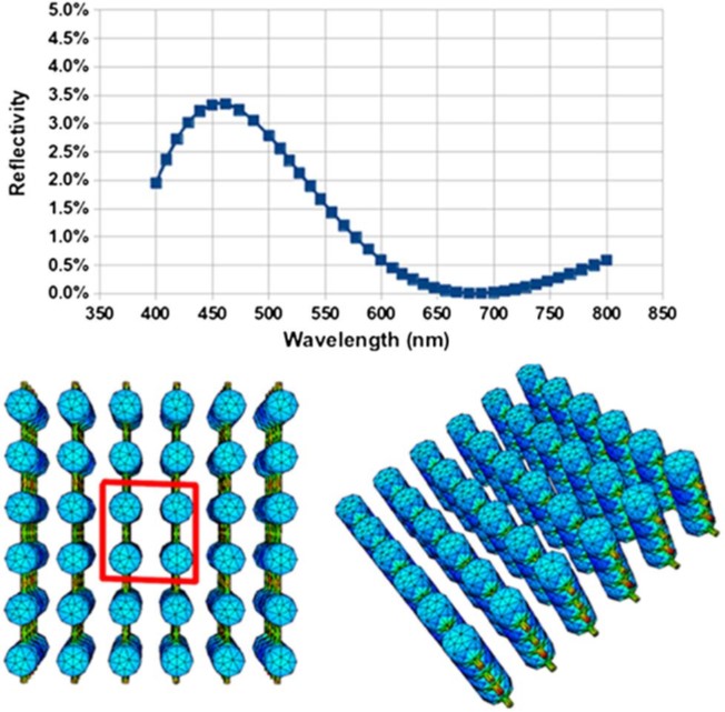
(Top) Calculated reflectivity of a single model butterfly scale. (Bottom) Scale geometry. A single square unit cell of side 320 nm is outlined in red. The height of the structure out of plane is 280 nm, and the diameter of the larger cylinders is 130 nm, with a center–center spacing of 160 nm between nearest neighbors. The smaller cylinders of diameter 20 nm with axes in the plane of periodicity are oriented along the polarization vector of the incident field, with a center–center spacing of 70 nm out of the plane of periodicity. The resultant mesh has N = 10,782. Average time to solution (without acceleration, extrapolated): ∼1430 min. Average time to solution (ACE acceleration): ∼31 min. Total speedup: ∼46×.
Transformation Optics Approach
Metamaterials (MM) and photonic crystals (PhCs) serve as the potential candidates for the experimental realization of transformational electromagnetic (T-E) devices.
A two-dimensional (T-E) device formed by configuring a circular disc with a Fermat spiral is realized. By tuning the phase of the emanating wave in the T-E medium, antenna switching and beam steering are made possible.
To simplify the permittivity and permeability tensors of the proposed T-E device, a gradient index approach is employed using purely dielectric material, which is then realized using photonic crystals (PhC).
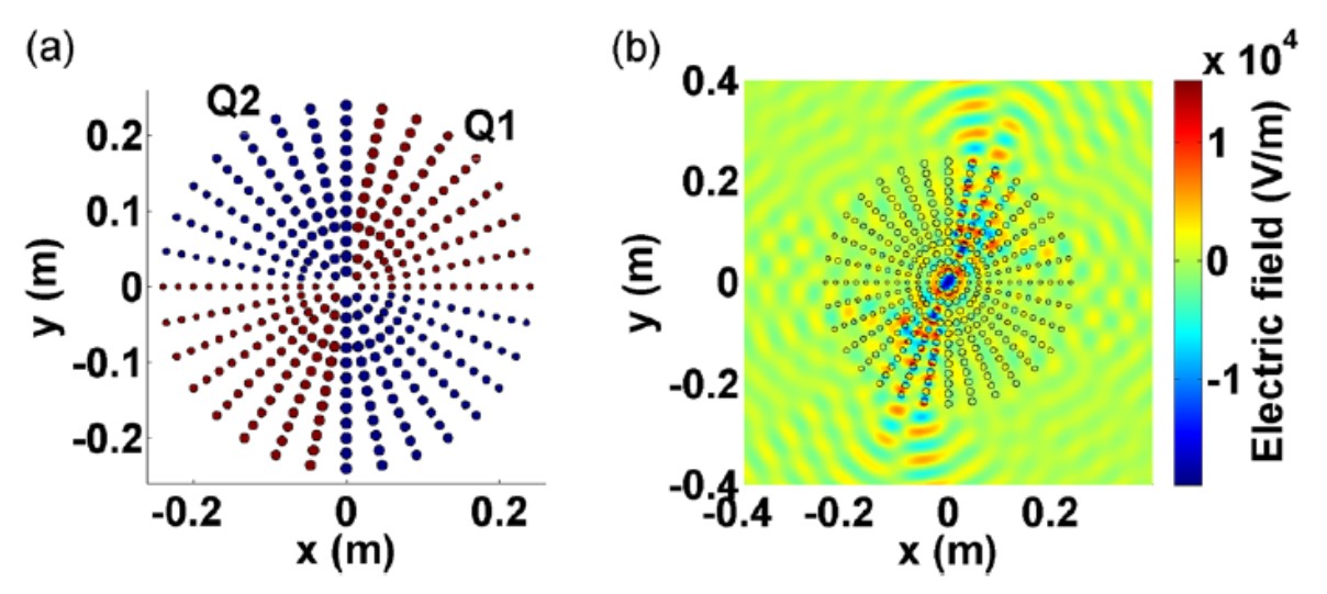
The GRIN PhC is made up of four wedges, where similar wedges occupy opposite quadrants. Wedge Q1 (red colour) and Q2 (blue colour) are placed in odd quadrants (I and III) and even quadrants (II and IV) respectively. Wedges Q1 and Q2 are made up of circular rods of permittivity 9 (Alumina) and 4.2 (Quartz glass) with a varying diameter as shown in Fig. (a). The arrangement provides a varying refractive index for the photonic crystal system to steer the beam along Fermat spiral. The lattice constant (a) of the GRIN PhC is 2 cm and radii of rods vary from 0.2a to 0.4a linearly at an interval a/40. Fig. (b) provides the electric field profile for a point source placed at the centre of the geometry.
Work flow
Novel Materials
The proposal seeks to develop novel materials that have widely differing electromagnetic properties through a spatial control over material composition.
Multiple fabrication techniques involving RF sputtering and electrospinning, along with chemical routes would augment additive manufacturing to produce complex geometrical structures involving low-loss as well as conductive composites, porous materials and sheet-like materials.

Beam Shapers
The proposal envisages the development of metamaterial lenses and metasurfaces in various transmit-receive configurations offering a wide scope of applicability.
Fabrication of these metamaterial components require additive manufacturing techniques involving a combination of metallic and polymeric materials.
- Engineered phase profiles
- Polarization control
- Frequency selectivity
- Wide acceptance angle
- Integrability with Antenna/Waveguide
- Compact
- Flexible
Absorbers
Absorbers are an integral part of devices in diverse areas spanning defense and civilian applications.
Absorbers are also increasingly used in energy harvesting technologies.
Goals
- Over 90% absorption efficiency
- Band selectability
- Sub-wavelength thickness
- Flexibility
- Ease of fabrication
- Cost effective
Challenges
- Impedance matching
- Creating complex 3-D layered structures
- Flexibility and Light weight
Approaches
- Creating complex surface currents
- Developing polymer composites
- Controlling penetration depths
- Developing material palette to suit additive manufacturing
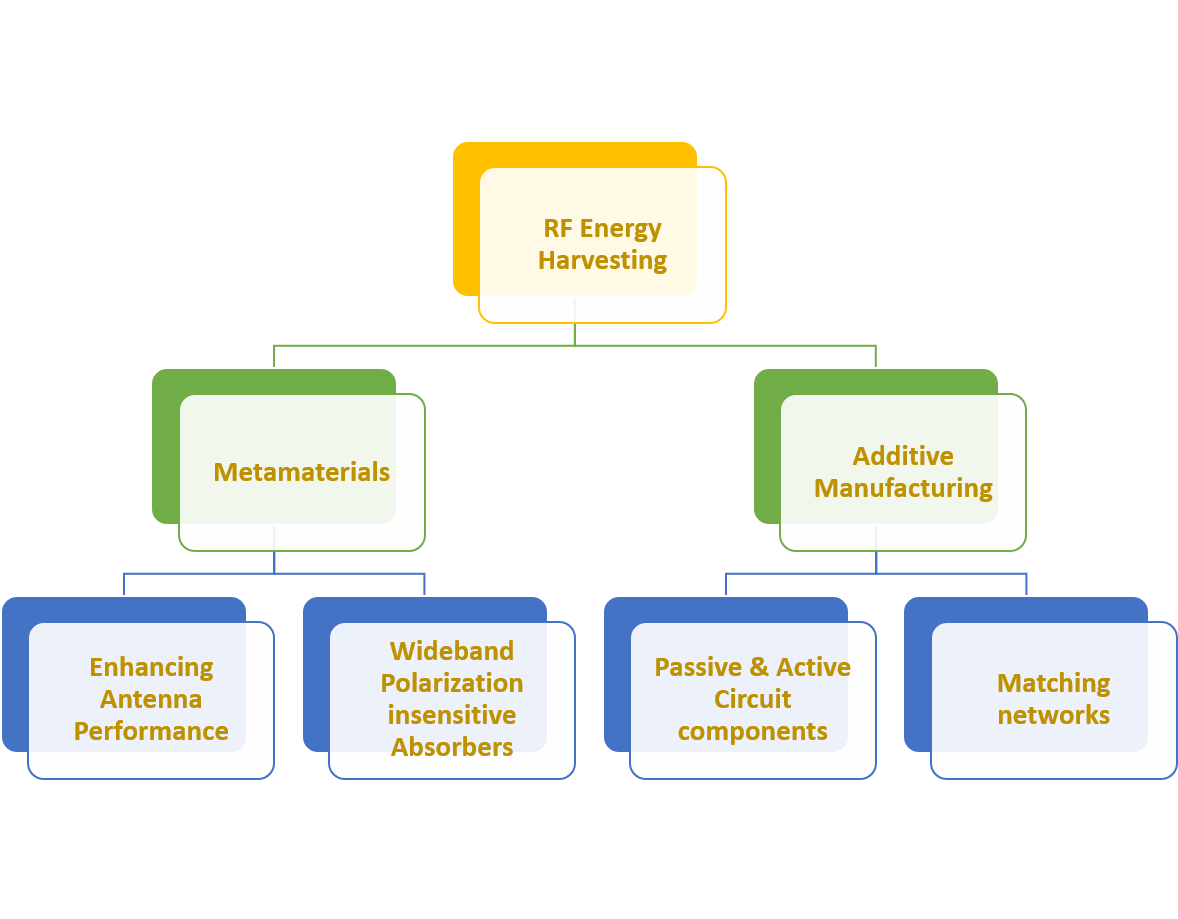
Energy Harvesting
With the growing need of different electromagnetic regions for communication purposes, there is plenty of scope to harvest energy from the ambient radiation.
Efficient harvesting requires the collection of broadband, polarization insensitive bursts of radiation over wide angles.
The proposal seeks to address these challenging requirements by exploiting the advantages offered by metamaterials at various stages of energy harvesting, and combining it with additive manufacturing processes to fabricate cost-effective, small foot-print circuits and matching networks. The feasibility of printing circuits on flexible substrates would be explored.
Sensors
Sensing is an integral part of the microwave system.
Improving the directivity, and increasing the gain of the antenna is useful for a variety of applications such as imaging and communication.
Small-foot print sensors, arrays, antennas with integrated feed and low-noise amplifier circuits are attractive in Non-Destructive Evaluation as well.
Challenges
- Planarity
- Thickness control when superstrates are used
- Multi-layer structures
Approaches
- Customized substrates
- Metamaterials as superstrates
- Metamaterial inspired antennas
- Designing with zero-index materials
Testing & Evaluation
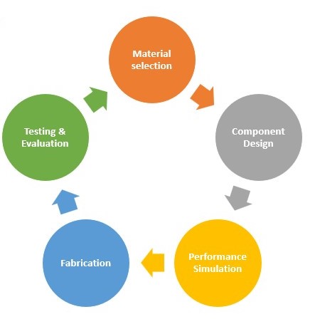
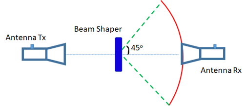
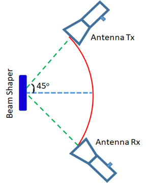
Facilities at the Microwave Lab such as the Anechoic chamber, standard gain antennas and VNAs would be used for characterizing materials and testing components. As the materials and components are envisaged to be engineered, evaluation would iterate between simulations and experiments. The evaluation of material properties at microwave and millimeter wave properties would be performed using reflection and transmission properties.
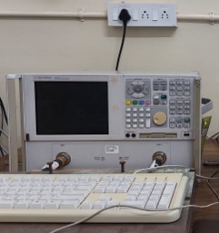
40 GHz VNA
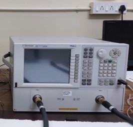
20 GHz VNA
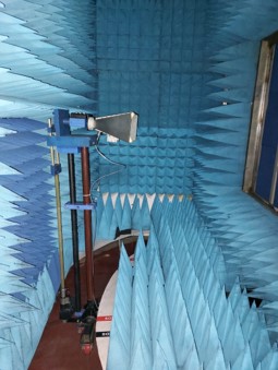
Customized Anechoic Chamber
One possible scheme involving transmission and reflection modes for evaluating a beam shaper is depicted.
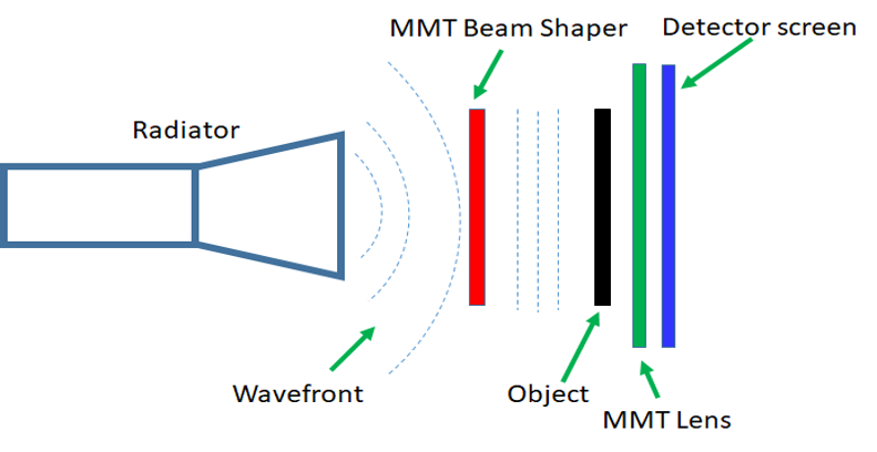
Imaging Material Properties
Material inhomogeneities arise from variations in density, dielectric permittivity and magnetic permeability.
For semi-transparent objects, spatial mapping of the inhomogeneities is proposed using non-contact modes of assessment.
An example scheme shown below depicts the use of an MMT beam shaper and an MMT lens for the mapping.
The detector screen consists of an array of sensors and could involve additively manufactured components.
Expected deliverables of the research
The project, with a total duration of 5 years.
Beam shapers, absorbers, and highly directive antennas would be developed for standalone applications. These elements would also be integrated into imaging and energy harvesting systems.
Current status
Procurement of equipments – Initiated Recruitment of manpower – Yet to be initiated
Collaborations
International Collaborations
Professor Shanker Balasubramaniam - Department of Computer science and Electrical Engineering, Michigan State University, USA
- Email: bshanker@egr.msu.edu
- Website
- Area of their expertise - Computational Electrodynamics
Professor Prem Chahal - Department of Computer science and Electrical Engineering, Michigan State University, USA
- Email: chahal@egr.msu.edu
- Website
- Area of their expertise
- Terahertz (THz) and Millimeter-wave Electronics
- IR Sensors
- Microsystems Packaging,
- RF-MEMS, BioMEMS, and Flex Electronics
- Additive Manufacturing
Industrial collaborations
External international site links for project
International education programs
It is planned to float a course for the master’s program. The course would be basically on the application of additive manufacturing for electromagnetic and acoustic metamaterials.
It is proposed to conduct two international conferences, titled, “Recent advances on the metamaterial-based devices at microwave and millimeter wave frequencies”, during the five year project period, one during the second year with special topics on microwave devices and next one during the fifth year with special emphasis on millimeter wave devices.
Societal impact
The outcomes from this project have potential applications in the health sector.
Sustenance statement
The strength of the proposal lies in the component-level development involving three activities, namely, material synthesis, metamaterial designs, and additive manufacturing, each of which offers a wide scope for innovation, application and extension.
The spin-offs anticipated from each of these activities is expected to provide scope for entrepreneurial activities given the strong and visible presence of the incubation cell at the IITM Research Park.
With the application potential of the proposal spanning across several sectors, collaborative ventures with industries would be actively pursued.
Technical/ Scientific Progress
New work done in the project
A new substrate has been made for designing a metamaterial-based microwave absorber. With this substrate, a metamaterial based microwave absorber has been designed, fabricated, and tested successfully.
Infrastructure developments
Thin film preparation unit and a ball-milling unit have been procured. The computational facility is being setup. As part of this facility, software licences have been procured and workstations are being procured.
Output
Journal publication: M. Anjali, Lincy Stephen, and V. Subramanian, Miniaturized metamaterial absorber based on a high permittivity substrate, Journal of Applied Physics 130, 113104 (2021); link
Mobility
Visits planned for PI, co-PIs, international collaborators and students (both inbound and outbound)
Relationship
Industrial Engagement
Currently working with a TATA Steel on developing Microwave absorber
University Engagement
Discussions are in progress.
Updates
Relevant Updates
Detailed work has been initiated in Metamaterial-based beam collimators involving Transformation Optics approach and Mie resonator based approach. In parallel, work on flexible microwave devices is in progress.