preloader

Photonic Integrated Circuits and Systems

Silicon Photonic Integrated Circuits and Systems: Design and Demonstration.

This project aims to demonstrate a working prototype of a multipurpose photonic integrated circuit chip suitable for microwave and quantum applications.

  • Development of SOI-based Tunable Basic Unit for Programmable Photonic Circuits : A tunable basic unit is the fundamental building block of programmable photonic circuits. Design, fabrication and characterization of the same using in-house technology is important to self-sufficient technology development.

  • Process Development of low-loss SiN Waveguide Technology : Low-loss SiN is a fast growing platform for photonic devices and circuits. Hence development of an optimised process line for the same is necessary.

  • Development of Semi-automated Characterization Facility : In order to characterize and test the fabricated devices and circuits, a fully equipped characterization facility is essential.

  • Development of Photonic Processor Chip : Design and development of a photonic processor chip prototype suitable for various applications is the primary goal of the project.

  • System-in-Package Photonic Chip : The packaging of photonic chips is a challenging task but very much essential for prototype and product development. A leading IC packaging industry, Si2 Microsystems, Bengaluru is in a tight collaboration for an efficient and cost-effective system-in-package solution.

Photonic Integrated Circuits and Systems

Prof. Bijoy Krishna Das

Principal Investigator

People


Project

Silicon photonics has been a booming area of research in the past couple of decades. Many application specific photonic integrated circuits (ASPICs) have been developed owing to standard CMOS fabrication compatibility of the silicon photonics technology. However, recent research focus has turned towards programmable photonic integrated circuits. Two important fields of application of such programmable photonic processors are Microwave photonics and Quantum photonics signal processings. Various passive and tunable devices have already been developed by our group in the previous years. Through this project, we propose to establish a Centre of Excellence on Photonic Integrated Circuits and Systems (PICS). The primary objective of the centre is to demonstrate a working prototype of the multipurpose programmable photonic processor core suitable for microwave as well as quantum photonic applications.

Expected deliverables of the research

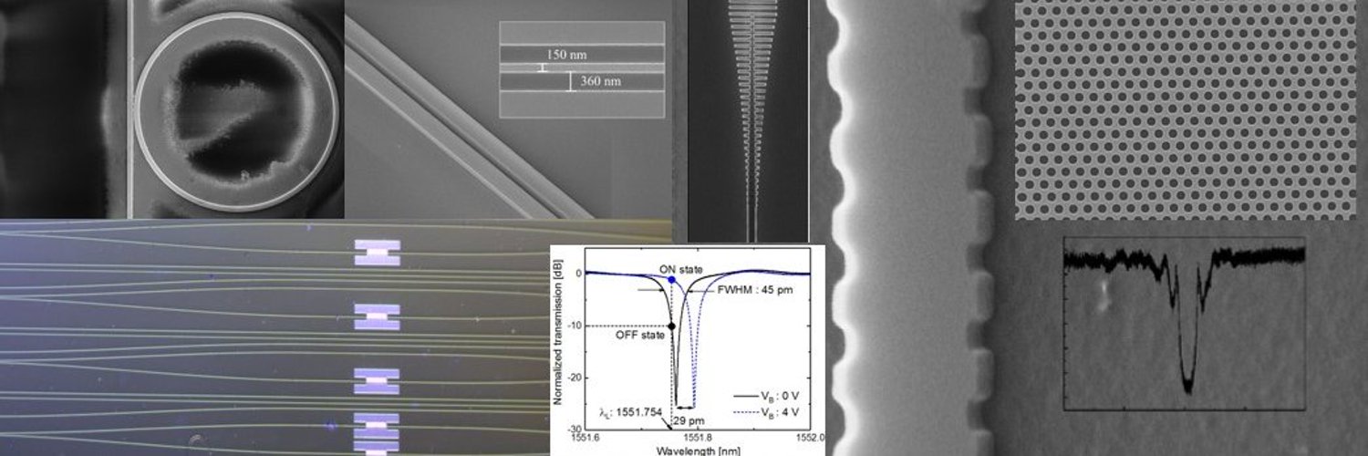
  • Design and demonstration of SOI based 2x2 MZI tunable basic unit (TBU) - the fundamental building block for programmable photonic integrated circuits.
  • Process development of low-loss SiN waveguide technology by leveraging existing facilities at the Centre for Nems and NanoPhotonics (CNNP), IIT Madras.
  • Photonic processor chip design and tape-out through multi-project wafer (MPW) runs
  • Electronic controller/driver chip design and tape-out.
  • Developing semi-automated characterization facility for fabricated photonics/electronics chips.
  • Fiber pigtailing and packaging of the fabricated chips in collaboration with Si2 microsystems and their testing.

Current status

  • Design and fabrication of SOI based MZI TBU in progress
  • Process development of SiN waveguide technology in progress
  • 1st chip design consisting of passive building blocks for a photonic integrated circuit has been sent to the foundry (AMF, Singapore) for tape-out.
  • The necessary upgradation of the existing e-beam lithography system has been completed - much needed for defining critical photonic integrated circuit components.
  • Procurement of equipment for characterization facilities in progress.
  • Photonics Chip Packaging rules are being developed with the collaboration of Si2 Microsystems, Bengaluru.

Collaborations

  • Prof. Jose Capmany Francoy

    • Chair in Photonics, ERC Advanced Grantee, IEEE and OSA Fellow, Photonics Research Labs Head, Universitat Politécnica de Valencia, Spain.
    • Email
    • Webpage
  • Prof. Wim Bogaerts

    • Photonics Research group, Ghent University, Belgium.
    • Email
    • Webpage
  • Prof. Shayan Mookherjea

    • Department of Electrical and Computer Engineering, University of California, San Diego, USA.
    • Webpage
  • Si2 Microsystems, Bengaluru.

  • iPronics, Programmable Photonics start-up, Spain.

Societal impact

The centre of excellence is proposed based on research outcomes and contributions in the area of silicon photonics during the last 14 years at IIT Madras, there is no hazardous societal impact except the promise of forward looking Make in India and Atmanirbhar Bharat in the domain of academic research and technology development. The immediate need of developing photonic integrated circuit technology is to accelerate wide-spread applications in the area of 5G/6G, Multi-band RADAR, QKD for secured communications systems, etc.

Sustenance statement

  • International collaborations bring in research collaboration as well as student/faculty exchange programs.
  • Induction of new faculty members to the core research team for multidimensional research outcomes and raising project funds from industry as well as from government agencies.
  • Besides creating IITM startups, collaboration with reputed industry partners have been planned for technology transfer and prospective commercialization of the prototype/product.

Visit our website for more details.