Analog, RF, and mixed-signal ICs form the basis for converting real-world signals into digital form, and storing, processing and transporting these signals.
1. Development and design of power-efficient precision delta-sigma converters: This effort seeks to achieve a step-change in this area (high-resolution and incremental delta-sigma converters), where the group has already made some headway. One example cited here is R. Theertham, P. Kootala, S. Billa and S. Pavan, Design considerations for continuous-time delta-sigma modulators with low in-band noise spectral density, IEEE Journal of Solid-State Circuits, September 2020.
2. Development and design of continuous-time pipelined ADCs for wide bandwidths: This aims to supplant discrete-time pipelined ADCs. While the prospects are promising, there are significant domain-specific signal-processing challenges to solve. This is a high-risk, high-reward effort with ground-breaking potential.
3. Development of area- and energy-efficient in-memory ADCs/DACs for AI/ML inference engines: This effort aims to push the envelope in power-efficient in-memory computing engines for AI/ML inference, an area of strong recent interest in machine-learning hardware.
4. Development of high-performance serial links (SERDES): The focus is on energy-efficient architectural and circuit-level techniques for serial links extended to 56 Gb/s, targeting fast-turn-on serial links for dynamic workloads, serial links for high-performance computing, and full-duplex wireline communication with reduced form factor.
5. Development of high-performance RF IC components: The goal is to realize widely tunable oscillators and frequency synthesizers with low phase noise, along with compact widely tunable delay lines. The group cites examples including a wide-tuning-range VCO presented at IEEE ISSCC 2019 and a widely tunable wideband delay line published in IEEE JSSC 2017.
(a) Delta-Sigma Data Converters and Incremental Delta-Sigma ADCs
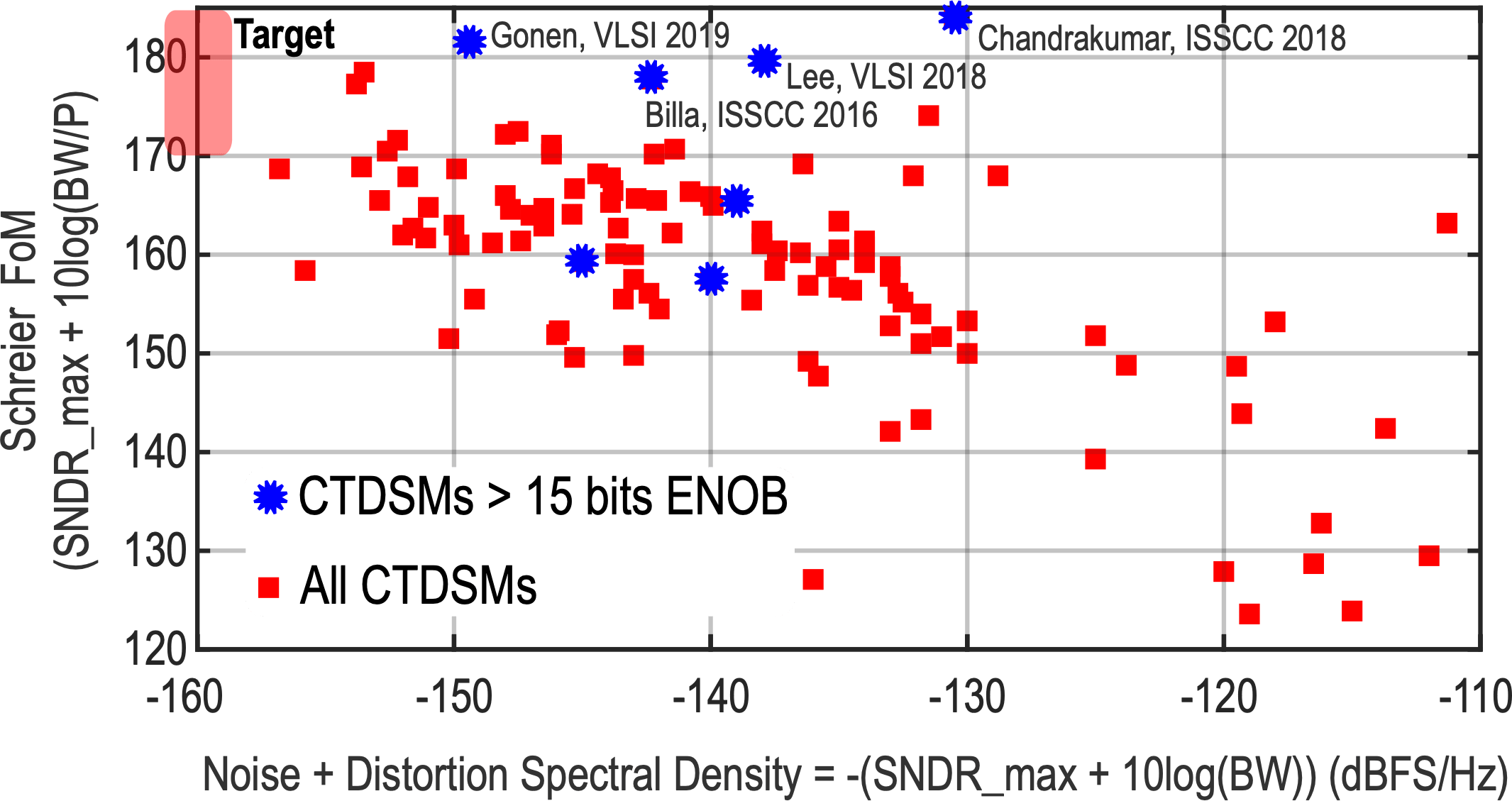
The area of precision data-conversion is not only commercially important, but is also a particularly challenging one. These tend to be done in legacy technologies (typically 180nm CMOS, now slowly moving to 130nm) as the signal bandwidths tend to be in the range of a few 10s of kHz to a few 100s of kHz. Continuous-time delta-sigma data converters (CTDSMs) are an attractive choice for the realization of high-resolution ADCs since they are easy to drive, and have implicit anti-aliasing. Thus, the signal chain is significantly improved. The adjoining figure (from AC and DC Data Acquisition Signal Chains Made Easy) compares the same signal chain realized using a conventional precision successive-approximation register (SAR) ADC, and a continuous-time delta sigma ADC. The latter eliminates a significant amount of peripheral circuitry (like antialias filters), saves power and occupies less than a third of the board space. However, several challenges remain in realizing arrays of precision ADCs, needed in several industrial automation applications. The reason is that achieving high resolution ( as characterised by the in-band signal-to-(noise + distortion) spectral density (NDSD) ) and high energy efficiency ( as quantified by the Schreier Figure-of-Merit ) has proved to be a very tough problem to crack. The figure below shows all the CTDSMs reported at two top conferences (ISSCC and VLSI Symposium) over the years.
The blue stars show CTDSMs that achieve a resolution of 15 bits or higher. We see that they all achieve a NSD greater than -150 dBFS. Some achieve good energy efficiency (higher Schreier FoM), but are restricted to kHz bandwidths. Our target is to achieve an in-band noise floor that is about an order of magnitude better than state-of-the art, while at the same time improving power efficiency, and reducing area. Both these aspects will enable us to pack multiple converter cores on the same die. The key challenges in realizing this are flicker noise and element mismatch in the feed-back DAC used in the converters. Over the last few years, we have made some headway in understanding and addressing these issues and the results have been published in top journals and conferences, as shown below.
R.Theertham, P.Koottala, S.Billa and S.Pavan, Design Techniques for High-Resolution Continuous-Time Delta-Sigma Converters With Low In-Band Noise Spectral Density " IEEE Journal of Solid State Circuits , September 2020.
R.Theertham and S.Pavan, Unified Analysis, Modeling, and Simulation of Chopping Artifacts in Continuous-Time Delta-Sigma Modulators ," IEEE Transactions on Circuits and Systems: Regular Papers, August 2019.
S.Billa, A.Sukumaran and S.Pavan,Analysis and Design of Continuous-time Delta-Sigma Modulators Incorporating Chopping," IEEE Journal of Solid-State Circuits, September 2017.
S.Pavan, Analysis of Chopped Integrators and its Application to Continuous-time Delta Sigma Modulator Design," IEEE Transactions on Circuits and Systems: Regular Papers, August 2017.
We would like to use our prior work as a base to further improve performance and introduce programmability in resolution and signal bandwidth in multichannel applications, where ADCs need to be shared among many multiplexed channels. Some of the key techniques that we have developed are likely to be extremely useful in the development of these particularly challenging applications.
(b) Continuous-Time Pipelined ADCs
The important domain of medium resolution, wide-bandwidth (10-12 bit, several 10s to 100s of MHz) ADCs has been dominated by discrete-time pipeline ADCs. Such ADCs, introduced in the early 1990s, and based on switched-capacitor principles are becoming increasingly problematic to design in advanced CMOS technologies with reduced supply voltages. This has led to extensive digital calibration of these converters that compensate for almost every analog impairment one can think of. In a practical system (like a wireless base-station) these ADCs need to be driven by an anti-alias filter. This makes it particularly challenging due to the switched-input capacitance load of such converters. Companies, therefore, resort to using an on-chip buffer that drives the switched-capacitor load. These buffers consume significant amounts of power and area.
A recent innovation in the area is the continuous-time pipeline ADC. The CTP has two primary advantages - it is easy to drive, as it presents a resistive input impedance, and it features inherent-antialiasing, which means that it is equivalent to having an ADC and the anti-alias filter rolled into one. We have been early movers in this area and we hope to make lasting contributions to this area.
H.Shibata, V.Kozlov, Z.Ji, A.Ganesan, H.Zhu, D. Paterson, J.Zhao, S.Patil and S.Pavan, A 9 GS/s 1.125 GHz BW Oversampling Continuous-Time Pipeline ADC Achieving -164 dBFS/Hz NSD," IEEE Journal of Solid-State Circuits, December 2017.
(c) In-memory Computing
The primary objective of this research program is to design and fabricate an Application Specific Integrated Circuit (ASIC) to infer conclusions from Deep Neural Networks(DNNs) while expending relatively low energy. Machine Learning(ML) systems, DNNs for example, have long been employed successfully in applications involving classification and regression, though all advances have been limited to software and mathematical theory. However in recent times big data, which refers to the large volume of raw data available from numerous sensors, has made computational hardware a relevant focus area in ML. Conventional methods were essentially limited to transferring raw data to a server/ cloud and employing high performance machines to process the data at high speeds with little optimization of power or energy consumption. Currently, with data being generated at petabytes per second, and the high cost and energy of data communication, there is a need to process data locally at/ near the sensor. Additionally, critical applications like the ones used in autonomous vehicles cannot afford the latency involved in transferring data to the cloud and back, in order to take a decision. Other applications may require high security and privacy. All of these drive the need for processing data locally in an energy efficient manner. DNNs like all ML systems has two modes of operation :- Training and Inference.
Training refers to learning a set of weights which minimizes the error on a known set of examples and is computationally very complex. Inference mode on the other hand is computationally less complex where data is presented to the DNN and output is the classified label. This project envisions the application where training of a DNN can happen off line in a central server/ cloud environment and the trained weights can be downloaded to the device of interest like the autonomous car or a mobile phone where the DNN will be operated solely in the inference mode. The proposal will be centered around ideas related to building an ASIC for optimizing the inference mode of a DNN from an energy and performance point of view. In the inference mode the computational bottleneck, from an energy perspective, is the Multiply Accumulate (MAC) operation where the inputs are multiplied with the stored weights and accumulated in a register. Traditional methods of data processing where storage (memory) is isolated from computing, expends most of the energy in fetching the weights from and writing results back to memory. In recent times, there has been a push to use memory not just to store data but also for computations and this field is known as In Memory Computing (IMC)
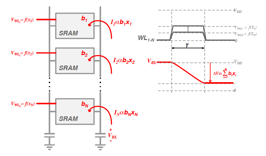
The basic idea of computing in memory is shown in the figure towards the left, where the circuitry in the SRAM is intelligently reconfigured for computing the matrix vector product. The input digital Xi is converted to an analog voltage (f(Xi)) with a Digital-to-Analog Converter (DAC) which in turn drives the word-line( WL). There are as many WL as there are inputs. The bit-line (BL) is driven high and then the WL turns on to allow current, proportional to biXi to flow through the access transistor. The current is equivalent to the multiply operation. Accumulation is achieved by turning on all the WLs together and hence the currents add along the BL. The BL voltage is the final MAC value but is in the analog domain. This analog quantity has to be converted into digital form. Evidently we see that data conversion is part and parcel of an IMC system. We require the following data converters for implementing an IMC engine:-
Digital to Analog Converter (DAC) - One per Word-line
Analog to Digital Converter (ADC) - One per Data-line (DL)
The application of these IMC ICs is primarily for computing on edge devices and that automatically imposes a constraint of having to be low energy. Further, the number of DACs and ADCs in the system decides the tradeoff between exploiting parallelism and reducing energy by completing the computation as soon as possible. To achieve the maximum parallelism we need one DAC per WL and one ADC per DL. Squeezing these data converters in the pitch of a row and column of an SRAM array, while expending as little energy as possible is a challenge.
Accordingly, the objectives of this proposal are the following. Design in-memory area- and power-efficient ADCs and DACs by reusing standard 6T or 8T SRAMcells. One aspect that can be exploited in IMC is the capability of calibrations. One idea that we would like to explore is an all digital in-memory calibration engine. The ideas of redundancy and error correction need to be explored. An alternative strategy to handling process variations is to use the idea of a Charge Trap Transistor (CTT) to shift the threshold voltage of the critical device in the memory cell by applying a high voltage on it’s GATE and if possible passing large current by applying an appropriate voltage across the drain and source.
High-Speed Serial Links
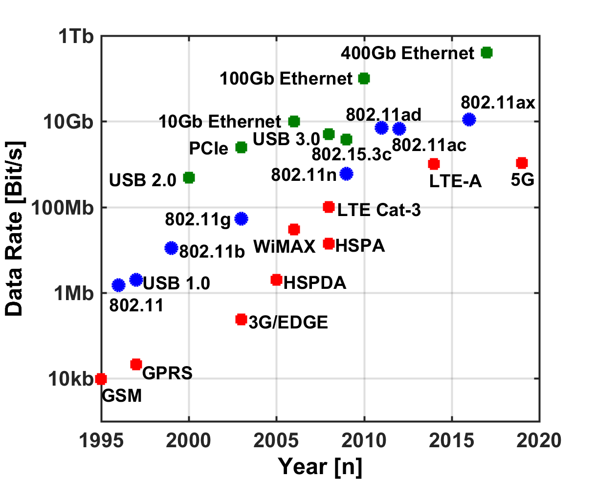
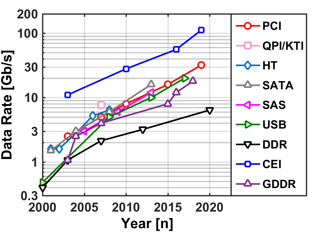
The increasing demand for data rates can be seen across wireless and wireline communication, both as depicted in technical trends in Fig. 1(i) published at the International Solid-State Circuits Conference (ISSCC 2020). Data rates have increased by more than three orders of magnitude over the last two decades. Wired data transfer between processing units and data-storage locations needs links with the maximum data rates. This is enabled by multiple wireline communication standards(Fig. 1(ii)).
(i)
(ii)
Figure 1. (i) Comparison between data rates for wireline and wireline communication standards. (ii) Per-lane transfer rates for different wireline communication standards. [1]
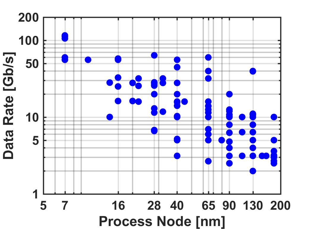
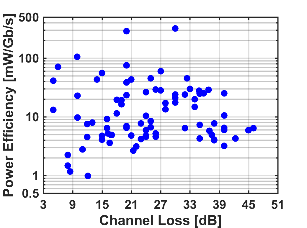
Technology has played a significant role in increasing data rates, as shown in Fig. 2(i). However, technology benefits are limited, and power consumption per bit transfer remains high at higher data rates due to increased channel loss (Fig. 2(ii)).
(i)
(ii)
Figure 2. (i) Data rates versus process node, (ii) power efficiency versus channel loss at Nyquist frequency for wireline transceivers. [1]
We categorize the research problems and elaborate on the methodology to execute the same in the next five years, given the energy-efficient wireline transceivers’ requirements.
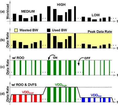
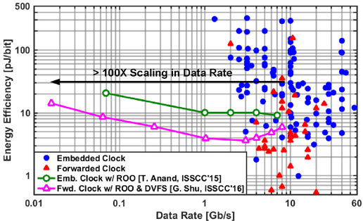
1. An energy proportional fast-on 0.56-56Gb/s serial link for dynamic workload environment
In data centers, the workload on processing units varies depending on user requirements, as depicted in Fig. 3(i). Typically, the data transfer links are always active irrespective of the processing requirements, thereby wasting the unused bandwidth. Techniques like rapid on/off and dynamic voltage and frequency scaling help to adapt serial links across data rates while matching the average bandwidth requirements for processing units. The energy efficiency of such links is compared with standalone transceivers in Fig. 3(ii). The figure shows the energy efficiency of serial links with embedded and forwarded clock architectures both. The standalone transceivers perform better than such reconfigurable links. But, the total energy consumed by such links leads to a waste of energy over a while. In this regard, we will explore design techniques to realize a 0.56-56Gb/s reconfigurable wireline transceiver while compensating a comparable channel loss. Currently, we are developing a 0.01-10Gb/s fast-on transceiver in the TSMC 65nm CMOS process. We will require advanced CMOS technology and newer design techniques to realize the proposed transceiver.
(i)
(ii)
Figure 3. (i) Rapid on/off (ROO) and dynamic voltage frequency scaling (DVFS) techniques for serial links in dynamic workload environment. (ii) Energy efficiency for serial links.]
2. A low power 56Gb/s serial link compensating >25dB channel loss
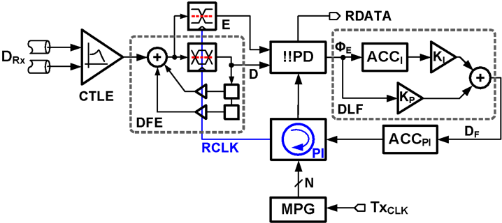
Figure 4. Block diagram of a high-speed wireline receiver.
Figure 2(ii) shows the power efficiency of serial links versus channel loss at Nyquist frequency. At higher data rates, channel loss is typically large and incurs a large power penalty. It leads to power efficiency around 10pJ/bit for channel loss greater than 25dB and data rates above 40Gb/s. The receiver hogs the power consumption due to its high-speed closed-loop operation. Figure 4 shows a block diagram of a typically employed phase interpolator based receiver. The receiver houses a continuous time linear equalizer (CTLE), decision feedback equalizer (DFE), and phase interpolator based digital clock and data recovery (CDR). DFE and CDR operate in closed-loop negative feedback and increase power consumption. Here, we will explore design techniques for energy efficient 56Gb/s transceiver with state-of-the-art performance.
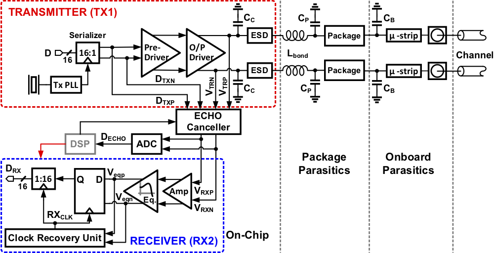
3. A low power 28-56Gb/s/pin full-duplex transceiver
Figure 5. A low power 28-56Gb/s/pin full-duplex transceiver
The aggregate IO bandwidth of multi-core processors is on ever-increasing demand. Increasing peak data rate per pin and full-duplex communication are two possible options to enhance the aggregate bandwidth without changing the form-factor. Figure 5 shows a block diagram of a full-duplex transceiver. In addition to a regular transmitter and receiver, it has an echo canceller and analog-to-digital converter (ADC). It helps cancel the transmitted signal and remove echo due to channel discontinuities, and recover the received bits error-free. It is often assisted by DSP units to calibrate echo cancellers. The challenge lies in realizing a full-duplex transceiver with a 2X per-pin data rate with an energy budget of two standalone transceivers with X data rate per-pin. The problem exacerbates with increased reflections at higher data rates. We aim to realize a low power 28-56Gb/s/pin full-duplex transceiver with novel circuit design and architectural level techniques.
In the research work proposed above, we target three serial link areas with application-specific requirements. Novel architecture and circuit-design techniques are required to reduce the power consumption in these applications. An advanced CMOS technology node will assist in achieving the lower power consumption and will be chosen accordingly.
D. C. Daly, L. C. Fujino and K. C. Smith, “Through the looking glass-2020 edition: Trends in solid-state circuits from ISSCC”, IEEE Solid-State Circuits Mag., vol. 12, no. 1, pp. 8-24, Jan. 2020.
Radio Frequency Integrated Circuits & Systems
Widely tunable low noise oscillators and frequency synthesizers
The proliferation of wireless standards in various bands scattered all over the spectrum has increased the need for voltage controlled oscillators (VCOs) and frequency synthesizers which cover a wide range. Oscillators using passive inductors and capacitors (LC VCOs) offer the best phase noise performance, but suffer from a narrow tuning range. Attempts to increase the tuning range by increasing the range of variation of capacitors invariably results in poorer phase noise. A promising approach is the use of multi-mode resonators which was demonstrated for GHz frequencies in [A]. Recent work in our group [B] has extended this technique to millimeter wave frequencies with a tuning range of 40%. A holy grail of sorts is a single oscillator that tunes over an octave range of frequencies. This permits the generation of any lower frequency
using integer division. We aim to achieve this without a significant area penalty by extending our earlier work. Another application of the widely tunable VCO stems from the following. Practical parameter constraints of CMOS processes enforce a “sweet spot” of performance in the 12-18GHz range. Below this frequency, inductors tend to have poorer quality factor and above this frequency switchable capacitor arrays tend to have a poorer quality factor. Often, to generate higher frequencies, a frequency synthesizer in this range is used as a reference to a second frequency synthesizer which doubles or triples the frequency. Octave range VCOs in the millimeter wave bands would enable continuous frequency coverage.
[A] G. Li et al., “A Low-Phase-Noise Wide-Tuning-Range Oscillator Based on Resonant Mode Switching,” IEEE JSSC, vol. 47, no. 6, pp. 1295-1308, June 2012.
[B] Abhishek Bhat and Nagendra Krishnapura, “A 25-to-38GHz, 195dB FoMT LC QVCO in 65nm LP CMOS Using a 4-Port Dual-Mode Resonator for 5G Radios,” 2019 IEEE International Solid- State Circuits Conference - (ISSCC), San Francisco, CA, USA, 2019, pp. 412-414.
Based on the above, we plan to demonstrate a single VCO that can tune over an octave range and a frequency multiplier using the VCO to obtain low phase noise at high frequencies. This work is also expected to result in interesting analysis of VCOs and their tuning techniques.
Wideband delay lines and beamforming arrays
Beamforming arrays provide directivity and gain by using multiple antennas. The larger the array, the more the benefits. But, larger arrays demand more delay lines, each with a longer delay(which must span the array size). Most high frequency delay lines are realized using passive inductors and capacitors. This results in a large size for the delay line and it is difficult to integrate a large beamforming array on a chip. Recent work in our group has demonstrated widely tunable wideband delay lines in the GHz range using 130nm CMOS process. We propose to extend it to frequencies exceeding > 10GHz using finer CMOS process. An associated problem is that, as components become smaller, mismatch between them increases resulting in group delay errors across the band which cause distortion in the beamforming patterns. These errors have to be corrected by calibration. Preliminary work in this direction showing the feasibility of both of the above has been carried out in the group.
Based on the above, we plan to demonstrate a delay line with a bandwidth of 8-10GHz with calibration for mismatch of active devices as well as a beamforming array using this delay line.
Expected deliverables of the research
Publications and Visible Output
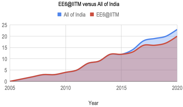
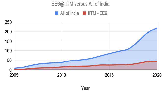
The top journals in the area are the IEEE Journal of Solid-State Circuits (JSSC), the IEEE Transactions on Circuits and Systems:Regular Papers (TCAS-1), the IEEE Solid-State CIrcuits Letters and the IEEE Transactions on Circuits and Systems:Express Briefs (TCAS-2). The IEEE Journal of Solid-State Circuits is particularly difficult to publish in, as one needs an interesting idea that needs to be proven with measurements on a fabricated chip. The figure below shows the number of papers published in the JSSC by our group over the last 15 years. 20 out of the 23 papers published in this journal from this country are from our work. Please note that IC design groups exist / have existed at all the old IITs and IISc for more than 15 years now.
IEEE JSSC papers from Indian academic groups
The IEEE Transactions on Circuits and Systems (TCAS-1 and 2) are the top venues to publish theory and analysis techniques in mixed-signal design. These journals have a much wider scope and many Indian groups publish here as seen in the figure below. Still, our group accounts for 20% of the papers in this journal. Similarly, the top conferences in the area are the International Solid-State Circuits Conference (ISSCC), the European Solid-State Circuits Conference (ESSCIRC), the Custom Integrated Circuits Conference (CICC), the International Symposium on VLSI Circuits (VLSI Symp.) and the Asian Solid State Circuits Conference (ASSCC). We are the first and only Indian group to have published at the ISSCC (with papers in ISSCC 2012, 2014, 2016, 2017, 2019). Two of us (Profs.Pavan and Krishnapura) have/are serving on the technical program committee of the ISSCC. To summarize, our group has a history of publishing in top places. We will continue to do that, and with CoE funding, should be able to scale up significantly. The deliverables will be in the form of high-performance IC prototypes and their characterization PCBs, and journal and conference papers in the top venues in the areas of Solid-State Circuits and Circuits-and-Systems.
IEEE TCAS papers from Indian academic groups
Manpower Development
The M.S program in Analog/Mixed-Signal design in collaboration with Texas Instruments India has been running for the past 10 years. This has proven to be fruitful to both TI and IITM - this program has not only resulted in extremely well-trained manpower for Indian industry, but also resulted in the solution of challenging and research-worthy industrial problems. This program is recognized across the country as being the “dream program” for students wishing to specialize in the analog area, with a very high bar of entry. Many of these students have done outstandingly well at Texas Instruments after being employed there.
The recently launched Web-enabled MTech program in VLSI is also a possible pipeline to attract bright students.
A majority of the 16 PhD students graduated from the group so far have either converted from the MS to the PhD program or have entered the PhD program directly after their bachelors degree.
Our three PhD students graduated from IIT-Madras are faculty at IIT-Delhi, IIT-Kanpur and IIT-Hyderabad. Two more will join academia soon.
Current status
Delta-Sigma Data Converters:
We have designed and fabricated several high-resolution data-converters that push the envelope in terms of performance, and others are being designed.
A.Baluni and S.Pavan, ``Analysis and Design of a 20 MHz Bandwidth Continuous-Time Delta-Sigma Modulator With Time-Interleaved Virtual-Ground-Switched FIR Feedback " IEEE Journal of Solid-State Circuits , March 2021.
S. Pavan, T.Halder and A.Kannan, “Continuous-Time Incremental Delta-Sigma Modulators with FIR Feedback”, IEEE Transactions on Circuits and Systems:Regular Papers, to appear
Continuous-time Pipeline ADCs:
A 100 MHz bandwidth prototype has been designed, fabricated and tested in a 65nm CMOS technology. Several next generation converter concepts are being investigated. Our recent publications in this area are the following.
S.Manivannan and S.Pavan, ``A 65nm CMOS Continuous-Time Pipeline ADC achieving 70dB SNDR in 100MHz Bandwidth" IEEE Solid-State Circuits Letters , May 2021.
S.Pavan and H.Shibata, ``Continuous-time Pipelined Analog-to-Digital Converters: A Mini-Tutorial" IEEE Transactions on Circuits and Systems: Express Briefs , March 2021.
In-memory Computing :
A Co-PI has two accepted conference paper, from IITM, where a proof of concept of an In-Memory flash ADC and IM-DAC were proposed
Balaji Vijaykumar and Janakiraman Viraraghavan: An Area-Efficient Word-Line Pitch-Aligned 8T SRAM Compatible Digital-to-Analog Converter, International Symposium on Circuits and Systems, 2021
Ashwin Balagopal and Janakiraman Viraraghavan: Flash Based In-Memory Multiply-Accumulate Realisation: a Theoretical Study, International Symposium on Circuits and Systems, 10-21 Oct 2020, Seville, Spain - Indian Patent Filed
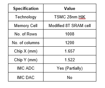
The Co-PI, along with his two research scholars, has taped out a chip in the TSMC 28nm technology and will complete testing the chip by the end of 2020. The details of the chip are as follows:-
Serial Links
A low-power 2.46-4.92GHz clock multiplier prototype has been tested and submitted for a journal publication. The clock multiplier achieves the lowest FoM1 -234.2dB for the largest clock multiplication ratio.
A 2.5-5.0GHz injection-locked clock multiplier with an embedded clock multiplier was published at a conference, and an Indian patent has been filed on the same.
A 0.01-10Gb/s fast-on voltage-mode transmitter with a fast-on low-power clock multiplier has been fabricated. The prototype is currently being tested.
An 8-16Gb/s/pin full-duplex transceiver is under development, and we will tape it out by June 2021.
Work on a 56Gb/s transceiver has been started.
Collaborations
International Collaborations
We have had international collaborations, mostly developed on an ad-hoc basis, with some top-international groups in the analog area. Examples of published work resulting from these collaborations include
University of Twente:
S.Pavan and E.Klumperink, ``Generalized Analysis of High-Order Switch-RC N-Path Mixers/Filters Using the Adjoint Network," IEEE Transactions on Circuits and Systems: Regular Papers, October 2018.
S.Pavan and E.Klumperink, ``Analysis of the Effect of Source Capacitance and Inductance on N-Path Mixers and Filters," IEEE Transactions on Circuits and Systems: Regular Papers, May 2018.
S.Pavan and E.Klumperink, ``Simplified Unified Analysis of Switched-RC Passive Mixers, Samplers, and N-Path Filters Using the Adjoint Network," IEEE Transactions on Circuits and Systems: Regular Papers, August 2017.
University of California, Los Angeles:
N.Sinha, M.Rachid, S.Pavan and S.Pamarti ``Design and Analysis of an 8 mW, 1 GHz Span, Passive Spectrum Scanner With >+31 dBm Out-of-Band IIP3 Using Periodically Time-Varying Circuit Components," IEEE Journal of Solid State Circuits, August 2017.
Analog Devices (High-speed converter group, Toronto):
H.Shibata, V.Kozlov, Z.Ji, A.Ganesan, H.Zhu, D. Paterson, J.Zhao, S.Patil and S.Pavan,``A 9 GS/s 1.125 GHz BW Oversampling Continuous-Time Pipeline ADC Achieving -164 dBFS/Hz NSD," IEEE Journal of Solid-State Circuits, December 2017.
Oregon State University and Analog Devices:
S.Pavan (IIT Madras), R.Schreier (Analog Devices) and G.Temes (Oregon State University), Understanding Delta-Sigma Data Converters, Wiley-IEEE Press, 2017.
Institute of Microelectronics, Sevilla (Spain), Chinese University of Hong Kong, Analog Devices:
Jose M de la Rosa, Richard Schreier, Kong-Pang Pun, Shanthi Pavan, “Next Generation Delta-Sigma Data Converters,” IEEE Journal on Emerging and Selected Topics in Circuits and Systems, Dec 2015.
University of Pavia, Italy:
Praveen M.V. , N. Krishnapura, M. Vallabhaneni and D. Manstretta, “A 11.7 dBm Output 1.9 GHz Power Mixer in a 0.13μm CMOS Process using Direct Current Sense Feedback based Transconductor,” 2018 International Solid State Circuits Conference (ISSCC) Student Research Preview, San Francisco, Feb 2018.
Industrial Collaborations
The PIs have had a long history of collaboration with companies.The M.S program in Analog/Mixed-Signal design in collaboration with Texas Instruments India has been running for the past 10 years. This has proven to be fruitful to both TI and IITM - this program has not only resulted in extremely well-trained manpower for Indian industry, but also resulted in the solution of challenging and research-worthy industrial problems. Many of these students have done outstandingly well at Texas Instruments after being employed there.
The PIs have also consulted for international companies like Vitesse Semi (USA), Ternetics (USA), Fairchild Semiconductor (USA) and spent summers at Analog Devices (Canada). Opportunities like this will continue to arise, and are primarily driven by the depth of our published work.
Technical/ Scientific Progress
New work done in the project
Designed and fabricated an In-Memory Computation chip in TSMC 28nm technology. Measurements are in progress.
Investigated low-pass and band-pass constant group-delay filters.
Design of low-noise and compact sub-sampling phase-locked loops.
Designed, fabricated and tested a two-stage cascaded 2.5-5.0GHz clock multiplier.
Designed an energy proportional 1-10Gb/s transmitter with a fast-on two-stage clock multiplier. The design is being fabricated.
Designed an 8-16Gb/s/pin full-duplex transmitter with time-based equalization and R-gm based near-end echo cancellation. The prototype is being tested.
Designed, fabricated and tested a 100MHz bandwidth, 12-bit Continuous-time pipelined ADC in a 65nm CMOS process.
An improved version, incorporating digital calibaration is being fabricated. New understanding of continuous-time pipelined ADCs and their sensitivity to component variations has been developed.
A precision, calibration-free, continuous-time delta-sigma converter achieving 17-bit performance in 250kHz bandwidth in a 180nm CMOS process has been designed, fabricated and tested.
Solved the long-standing problem of understanding (in)stability of incremental delta-sigma modulators with FIR feedback, and developed a solution to address this problem.
Infrastructure developments
CAD tools for IC design, tunable passive filters for testing have been ordered.
Output
B. Vijayakumar and J. Viraraghavan, “An Area-Efficient Word-Line Pitch-Aligned 8T SRAM Compatible Digital-to-Analog Converter,” 2021 IEEE International Symposium on Circuits and Systems (ISCAS), 2021, pp. 1-5, doi: 10.1109/ISCAS51556.2021.9401131.
R. S. A. Kumar and N. Krishnapura, “Multi-Channel Analog-to-Digital Conversion Using a Delta-Sigma Modulator Without Reset and a Modulated-Sinc-Sum Filter,” IEEE Transactions on Circuits and Systems I: Regular Papers, 2022. (doi: 10.1109/TCSI.2021.3094679).
A. Bhat and N. Krishnapura, “A Reduced-Area Capacitor-Only Loop Filter With Polarity-Switched Gm for Large Multiplication Factor Millimeter-Wave Sub-Sampling PLLs,” IEEE Transactions on Circuits and Systems I: Regular Papers, 2022, (doi: 10.1109/TCSI.2021.3096843).
Chithra, A. Narayanan, R. S. A. Kumar and N. Krishnapura, “Auto-Zeroing Static Phase Offset in DLLs Using a Digitally Programmable Sensing Circuit,” in IEEE Transactions on Circuits and Systems II: Express Briefs, vol. 68, no. 6, pp. 1788-1792, June 2021.
IRIS webinar on 22 October
G. R, J. D. Bandarupalli, and S. Saxena, “Injection-locked clock multiplier
with embedded phase interpolator,” Indian Patent App. No. 202141019940."
“Invited talk at the Forum on “Pushing the frontiers in Accuracy in Data Converters and Analog Circuits” at the International Solid State Circuits Conference (ISSCC), San Francisco (Virtual due to COVID) 2021. The talk was titled “"“Architectural and Design Challenges in High-Resolution Continuous-Time Delta-Sigma Data Converters”.
Invited Talk at the Workshop Deep Analysis Can Compress the Time to Design Optimum Analog/Mixed-Signal Circuits at the Symposium on VLSI Circuits, Kyoto, Japan (Virtual due to COVID).
Indian Patent 373933, Low Distortion Filters, S.Pavan and S.Viswanathan.
Indian Patent 374431, Method and Apparatus for Low Power Delta-Sigma Modulation. S.Pavan.
Analysis of RC Time-Constant Variations in Continuous-Time Pipelined ADCs
S Pavan, S Manivannan
IEEE Transactions on Circuits and Systems I: Regular Papers (to appear in 2022)
Alias Rejection in CT Delta-Sigma ADCs Using Virtual-Ground-Switched Resistor Feedback
R Theertham, S Pavan
IEEE Transactions on Circuits and Systems II: Express Briefs
Continuous-Time Incremental Delta-Sigma Modulators With FIR Feedback
S Pavan, T Halder, A Kannan
IEEE Transactions on Circuits and Systems I: Regular Papers
A 28.5 µW All-Analog Voice-Activity Detector
U Mukherjee, T Halder, A Kannan, S Ghosh, S Pavan
2021 IEEE International Symposium on Circuits and Systems (ISCAS)
A 65-nm CMOS Continuous-Time Pipeline ADC Achieving 70-dB SNDR in 100-MHz Bandwidth, S Manivannan, S Pavan, IEEE Solid-State Circuits Letters 4, 92-95
Analog-to-digital convertor (ADC) with a synthesized delay stage
Shanthi Pavan Yendluri and Hajime Shibata, US Patent US10958281B1
Analysis and Design of a 20-MHz Bandwidth Continuous-Time Delta-Sigma Modulator With Time-Interleaved Virtual-Ground-Switched FIR Feedback, A Baluni, S Pavan, IEEE Journal of Solid-State Circuits, March 2021.
Continuous-time pipelined analog-to-digital converters: A mini-tutorial,
S Pavan, H Shibata, IEEE Transactions on Circuits and Systems II: Express Briefs 68 (3), 810-815
Mobility
Visits planned for PI, co-PIs, international collaborators and students (both inbound and outbound)